Semiconductor device and method of manufacturing the same

a semiconductor and device technology, applied in semiconductor devices, transistors, electrical devices, etc., can solve the problems of reduced device size, difficult to partially check the upward expansion, and difficulty in reducing the size of the devi

Active Publication Date: 2009-11-17
SEMICON COMPONENTS IND LLC
View PDF57 Cites 8 Cited by
  • Summary
  • Abstract
  • Description
  • Claims
  • Application Information

AI Technical Summary

Benefits of technology

[0013]Moreover, the semiconductor device of the present invention includes, in a region to which the first buried diffusion layer of the one conductivity type has expanded upward, the second buried diffusion layer of the one conductivity type is formed in an overlapping manner. Accordingly, in the present invention, the first diffusion layer of the one conductivity type is connected to a region in which the first and second buried diffusion layers overlap each other, so that a collector resistance can be reduced.
[0014]Furthermore, the semiconductor device of the present invention includes the first diffusion layer of the one conductivity type is connected to the first buried diffusion layer of the one conductivity type, and in the connecting region, the second buried diffusion layer of the one conductivity type is formed. Accordingly, in the present invention, a region to which the first buried diffusion layer of the one conductivity type expands upward is used as a connecting region for the collector region. The first buried diffusion layer of the one conductivity type can be confined, and the width of lateral diffusion thereof can also be reduced.
[0017]Moreover, the method of the present invention includes, before implanting the ions of the impurity to form the second buried diffusion layer of the opposite conductivity type, the step of thermal oxidization is performed on the semiconductor substrate. Accordingly, in the present invention, with an impurity concentration in the surface of the first buried diffusion layer of the one conductivity type and in the vicinity of the surface, ions of an impurity of the opposite conductivity type are implanted. With this method, the upward expansion of the first buried diffusion layer of the one conductivity type can be checked. Additionally, when forming the epitaxial layer, the autodoping of an impurity of one conductivity type can be confined.
[0018]Furthermore, the method of the present invention includes, between the step of thermal oxidation and the step of implanting the ions of the impurity to form the second buried diffusion layer of the opposite conductivity type, the step of thermal processing in a non-oxidizing atmosphere is not performed. Accordingly, in the present invention, by implanting the ions of the impurity of the opposite conductivity type into a region in which the concentration of the impurity of the one conductivity type has become low, the second buried diffusion layer of the opposite conductivity type can be effectively formed.

Problems solved by technology

On the other hand, in the control NPN transistor, there is the following problem.
When the film thickness of the epitaxial layer is increased, an isolation region is extended in the lateral direction, and thus it is difficult to reduce a device size.
That is, the monolithic formation of the power vertical PNP transistor and the control NPN transistor causes a problem in which the breakdown voltage characteristics of the power vertical PNP transistor and the reduction in the device size of the control NPN transistor are in a trade-off relationship.
However, even for the P type buried diffusion layer which is located under the silicon nitride film, a wraparound by oxygen, or the like, causes a problem that it is difficult to partially check the upward expansion.
Accordingly, in order to satisfy desired breakdown voltage characteristics, it is necessary to form epitaxial layers of a two-layer structure, thus causing a problem that the manufacturing costs are increased.
However, in some cases, the silicon nitride film is not formed in a desired region over the P type buried diffusion layer due to the displacement of a mask or the like which occurs when the silicon nitride film formed on the epitaxial layer is selectively removed.
In such a case, a region where the P type diffusion layer overlaps the P type buried diffusion layer is reduced, and thus a collector resistance cannot be reduced.
Accordingly, a manufacturing process is complicated.
When forming epitaxial layers, there is a problem that boron (B), which is a P type impurity diffused over the semiconductor substrate, tends to be easily auto-doped.

Method used


Image

  • Semiconductor device and method of manufacturing the same
  • Semiconductor device and method of manufacturing the same
  • Semiconductor device and method of manufacturing the same

Examples


Embodiment Construction

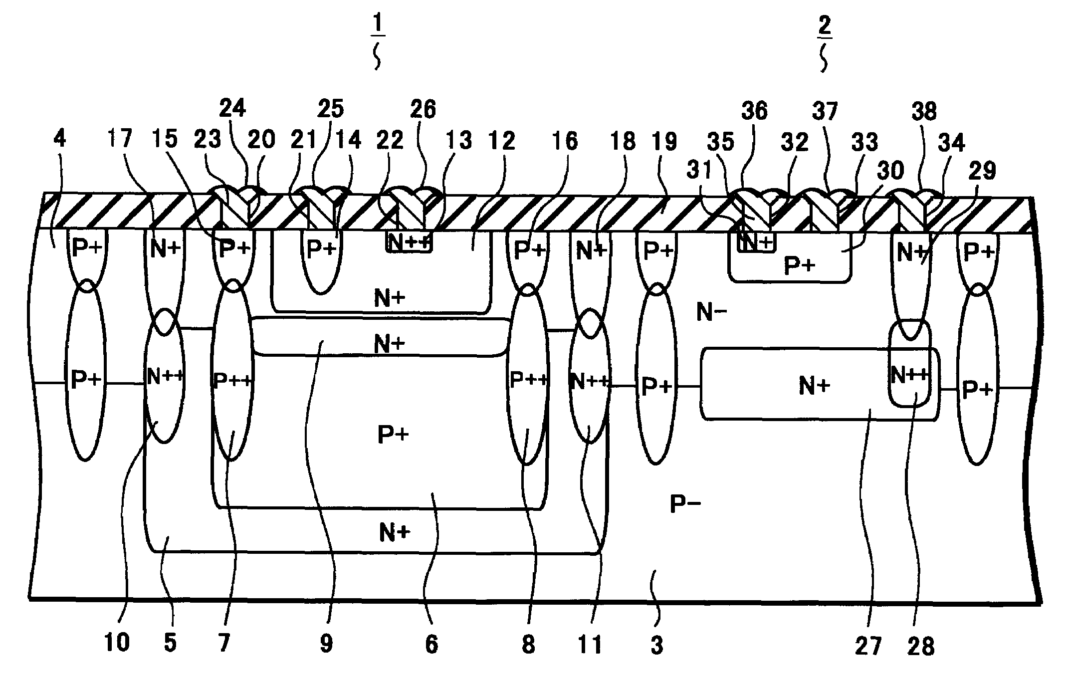
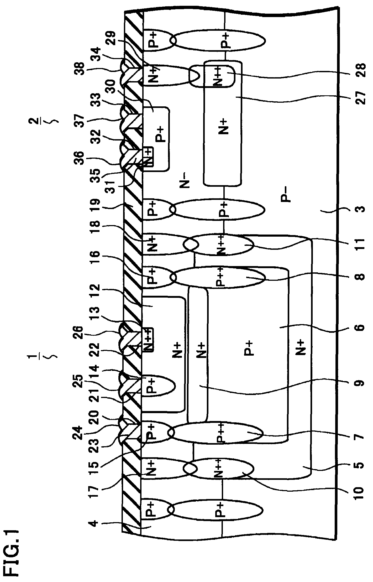
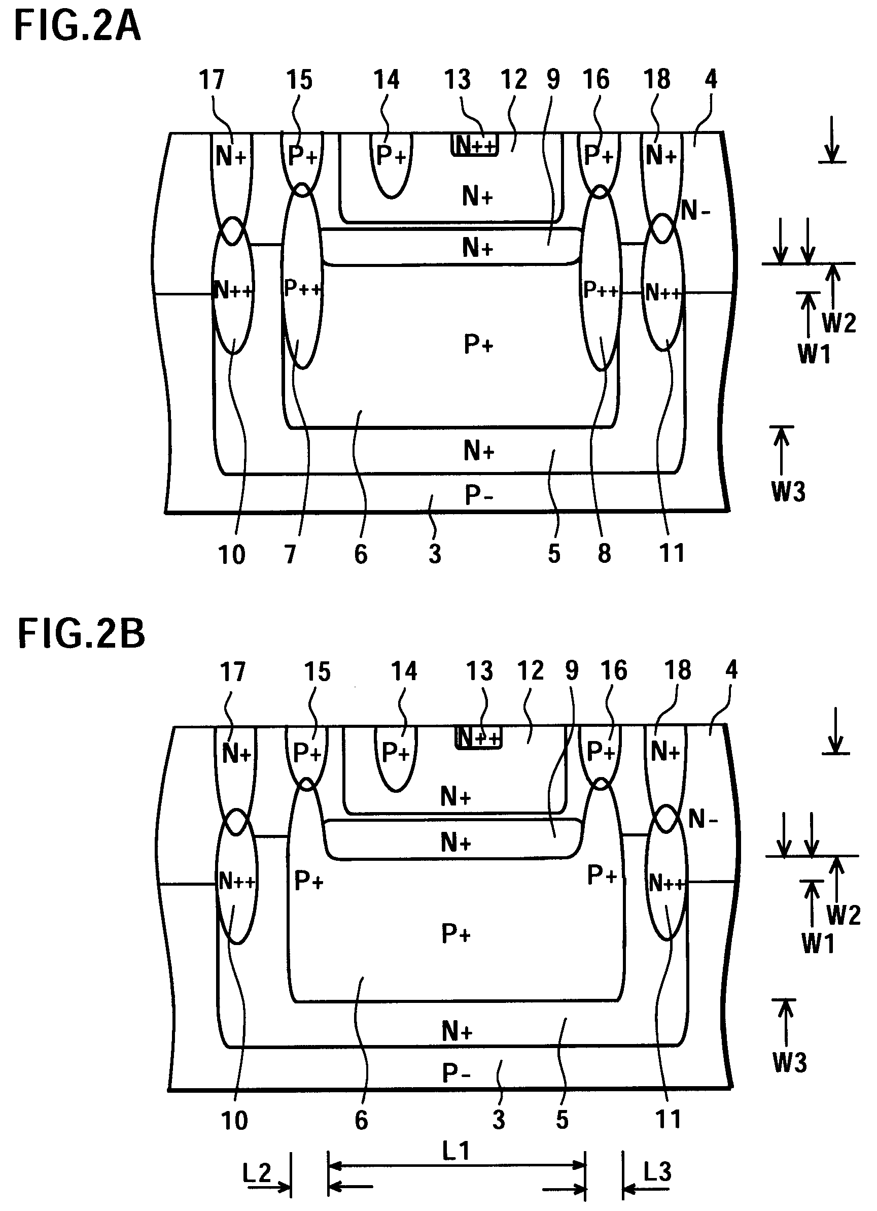
[0030]An embodiment of a semiconductor device of the present invention is described below in detail with reference to FIGS. 1 to 3. FIG. 1 is a sectional view for describing a semiconductor device of the present embodiment. FIG. 2A is a sectional view for describing a vertical PNP transistor of the present embodiment. FIG. 2B is a sectional view for describing a vertical PNP transistor of the present embodiment. FIG. 3A is a graph for describing the sheet resistance value and the width of the upward expansion of a buried diffusion layer of the semiconductor device of the present embodiment. FIG. 3B is a graph for describing the breakdown voltage characteristics of the semiconductor device of the present embodiment.

[0031]As shown in FIG. 1, a vertical PNP transistor 1 and a vertical NPN transistor 2 are monolithically formed on a P type single crystal silicon substrate 3. For example, the vertical PNP transistor 1 is used as a power semiconductor element, and the vertical NPN transis...


PUM


Abstract

In a semiconductor device of the present invention, an N type epitaxial layer is formed on a P type single crystal silicon substrate. In the substrate and the epitaxial layer, an N type buried diffusion layer is formed on a P type buried diffusion layer. With this structure, an upward expansion of the P type buried diffusion layer is checked and a thickness of the epitaxial layer can be made small while maintaining the breakdown voltage characteristics of a power semiconductor element. Accordingly, a device size of a control semiconductor element can be reduced.

Description

BACKGROUND OF THE INVENTION[0001]Priority is claimed to Japanese Patent Application Number JP2005-345504 filed on Nov. 30, 2006, the disclosure of which is incorporated herein by reference in its entirety.[0002]1. Field of the Invention[0003]The present invention relates to a semiconductor device and a method of manufacturing the same, which reduce a collector resistance of a vertical PNP transistor used as a power semiconductor element.[0004]2. Description of the Related Art[0005]As an embodiment of a method of manufacturing a conventional semiconductor device, a method of manufacturing the following vertical PNP transistor has been known. A P type semiconductor substrate is prepared, and two N type epitaxial layers are formed on the substrate. An N type buried diffusion layer is formed so as to extend in the P type semiconductor substrate and a first epitaxial layer, and a P type buried diffusion layer is formed so as to extend in the first and second epitaxial layers. Then, a sil...

Claims


Application Information

Patent Timeline
Patent Type & Authority Patents(United States)
IPC IPC(8): H01L29/08H01L29/732H01L21/8222H01L21/8228
CPCH01L21/82285H01L27/0826H01L29/1012H01L29/735H01L29/66272H01L29/7322H01L29/6625H01L21/761H01L21/38H01L21/8224
Inventor MITA, KEIJIOOKA, KENTARO
Owner SEMICON COMPONENTS IND LLC
Why Eureka
Try Eureka