SiGe hbt single tube structure, its manufacturing method and SiGe hbt multi-finger structure

A single-tube structure, germanium-silicon technology, used in semiconductor/solid-state device manufacturing, electrical components, circuits, etc., can solve the problems of large active area size, high doping concentration, large spacing distance, etc., and reduce collector resistance. , the effect of large output power and power gain

Active Publication Date: 2016-02-10
SHANGHAI HUAHONG GRACE SEMICON MFG CORP
View PDF6 Cites 0 Cited by
  • Summary
  • Abstract
  • Description
  • Claims
  • Application Information

AI Technical Summary

Problems solved by technology

[0003] Although this process technology is mature and stable, its main disadvantage is that in order to reduce the collector resistance, the size of the active region is large and the doping concentration is high. In order to avoid lateral diffusion affecting the release of impurities in the active region of the device, two The distance between the active regions needs to be larger, so that the overall device is larger, the parasitic capacitance of the base-collector region, and the capacitance of the collector region-silicon substrate are also larger

Method used


Image

  • SiGe hbt single tube structure, its manufacturing method and SiGe hbt multi-finger structure
  • SiGe hbt single tube structure, its manufacturing method and SiGe hbt multi-finger structure
  • SiGe hbt single tube structure, its manufacturing method and SiGe hbt multi-finger structure

Examples


Embodiment Construction

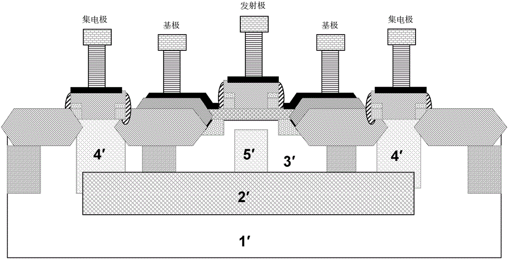
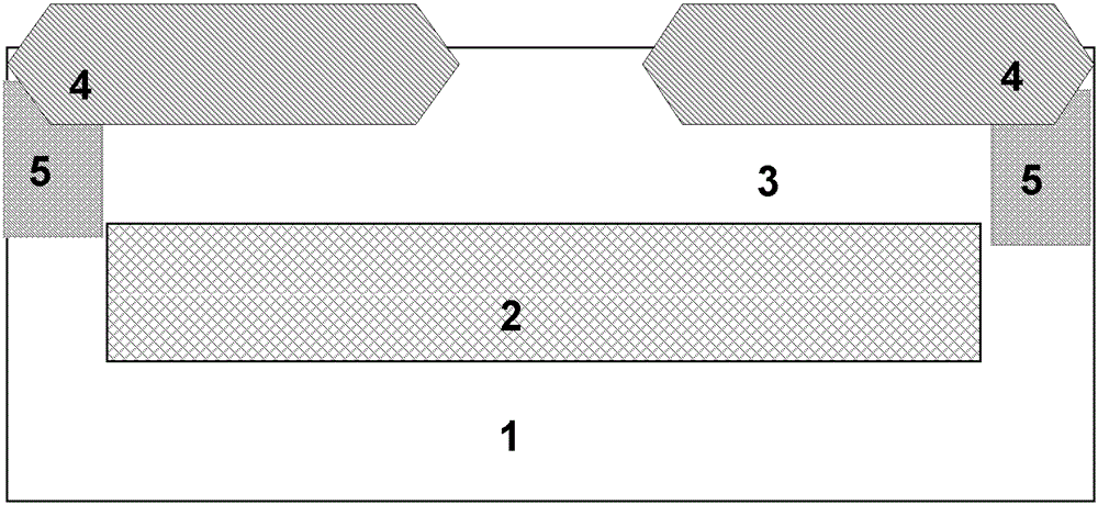
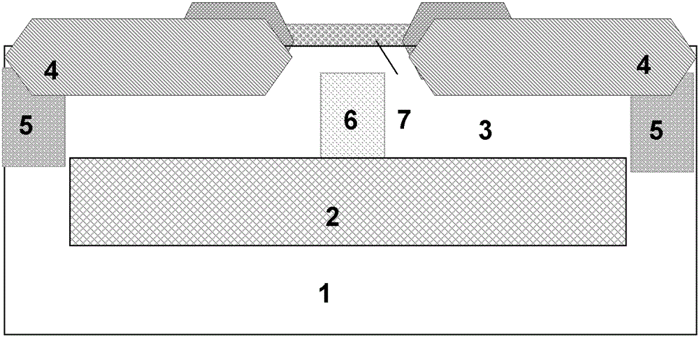
[0050] The manufacturing method of silicon germanium HBT single tube structure of the present invention comprises the following steps:

[0051] Step 1, carry out high dose (10 15 cm -2 ~10 16 cm -2 ), medium-energy (50KeV~100KeV) N-type ion implantation, high-temperature annealing after implantation, the temperature is between 1050°C and 1150°C, and the annealing time is more than 60 minutes to form a low-resistance N-type buried layer 2 channel, implant The ion is preferably arsenic, which is heavy enough to prevent further diffusion during the subsequent annealing process without causing significant damage to the silicon substrate;

[0052] Step 2, perform low N-doped epitaxial growth on the N-type buried layer, the thickness is between 0.8 μm and 2.0 μm, and the doping concentration is 10 15 cm -3 ~10 16 cm -3 ;

[0053] Step 3: Perform medium and high doses (10 14 cm -2 ~5×10 15 cm -2 ), medium-energy (50keV~200keV) P-type ion implantation to form a P-type ion ...


PUM


Abstract

The invention discloses a germanium-silicon heterojunction bipolar transistor (HBT) single tube structure. A collector region C is manufactured through a low-doping N type epitaxy technique, and the bottom of the collector region C is extracted by a heavy N type doping buried layer; a base region B is composed of a boron heavy doping germanium-silicon epitaxial layer; a transmitting region E is formed by etching media deposited on the base region to form a window and then depositing N type doping polycrystalline silicon; an N type epitaxy at the bottom of field oxide under outer base region polycrystalline silicon is converted to a P type region through P type ion injection and high-temperature annealing; and a collector electrode is extracted by a deep groove contact hole and metals. The invention further discloses a multi-finger structure in a CBEBE...BEBC or CEBECBE...CEBEC mode. The deep groove contact hole penetrates through the field oxide and the N type epitaxy to penetrate into the N type buried layer, the space of two transmitting electrodes can be greatly reduced, the collector resistance of device is reduced, and junction capacitance of the collector electrode for the base region and a silicon substrate is reduced. A P type ion injection region is not communicated with a P type ion injection region arranged outside the device, so that base electrode-collector electrode medium capacitance is reduced. The multi-finger structure can obtain the largest output power and power gain.

Description

technical field [0001] The invention relates to the field of semiconductor integrated circuits, in particular to a germanium-silicon HBT single-tube structure. The invention also relates to a manufacturing method of the silicon-germanium HBT single-tube structure, and a silicon-germanium HBT multi-finger structure formed from the single-tube structure of the silicon-germanium HBT. Background technique [0002] Conventional germanium-silicon heterojunction bipolar transistors such as figure 1 As shown, the formation of the collector electrode is as follows: high-dose N-type ion implantation is performed on the P-type substrate 1′, and high-temperature annealing is performed after implantation to form an N-type low-resistance buried layer channel 2′, followed by low N-doping The epitaxial growth 3', and then perform selective N-type ion implantation 5' under the emitter window to form a low-resistance seat, and finally perform high-dose N-type ion implantation in another acti...

Claims


Application Information

Patent Timeline
Patent Type & Authority Patents(China)
IPC IPC(8): H01L29/06H01L29/737H01L21/331
Inventor 周正良李昊
Owner SHANGHAI HUAHONG GRACE SEMICON MFG CORP
Why Eureka
Try Eureka