Heterojunction bipolar transistor

a bipolar transistor and junction technology, applied in the direction of basic electric elements, electrical equipment, semiconductor devices, etc., can solve the problems of reducing affecting unable to effectively achieve the effect of improving the efficiency of dhbts, so as to improve the efficiency of power amplifiers, reduce collector resistance, and increase output

Active Publication Date: 2020-09-15
MURATA MFG CO LTD
View PDF8 Cites 1 Cited by
  • Summary
  • Abstract
  • Description
  • Claims
  • Application Information

AI Technical Summary

Benefits of technology

[0010]Accordingly, the present disclosure provides an HBT capable of suppressing a decrease in the linearity of input-output characteristics thereof.
[0022]The collector resistance can be reduced. As a result, higher output and an improvement in the efficiency of a power amplifier including a heterojunction bipolar transistor can be realized.

Problems solved by technology

The effect of improving the efficiency of DHBTs may not be effectively achieved due to this blocking effect.
The decrease in the linearity of Cbc-Vbc characteristics results in degradation of an adjacent channel leakage ratio (ACLR), which is an index representing the distortion of power amplifiers.

Method used


Image

  • Heterojunction bipolar transistor
  • Heterojunction bipolar transistor
  • Heterojunction bipolar transistor

Examples


first embodiment

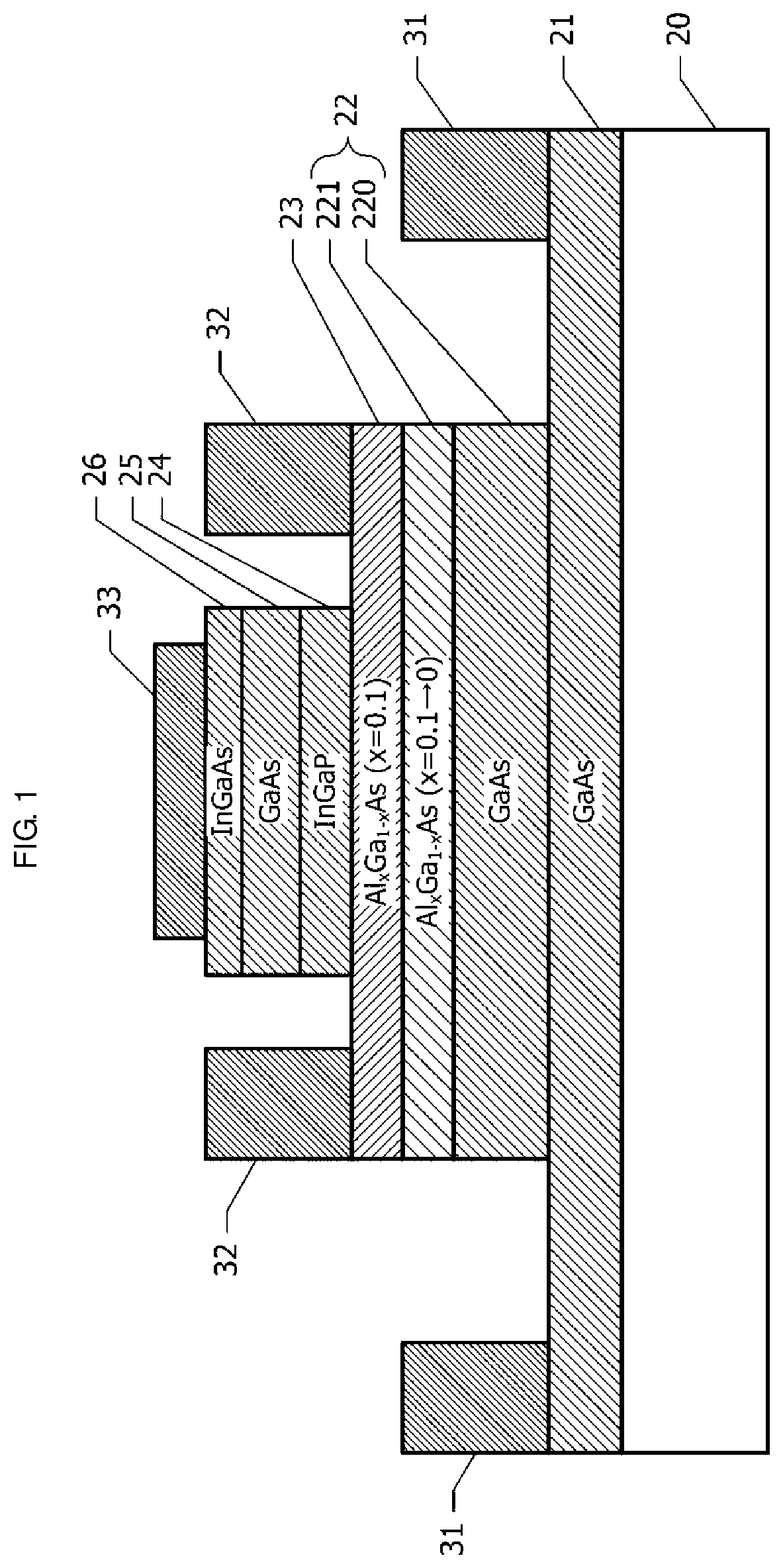
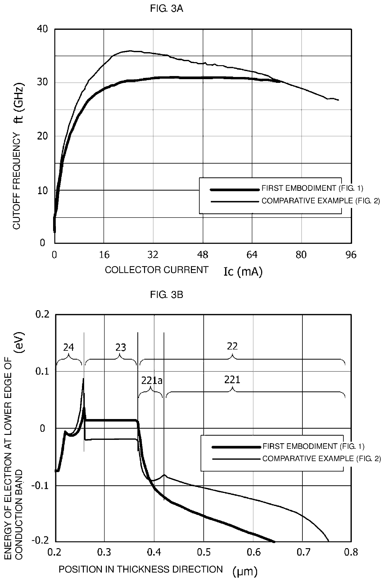
[0040]An HBT according to a first embodiment will be described with reference to FIGS. 1 to 3B.

[0041]FIG. 1 is a sectional view of an HBT according to the first embodiment. A sub-collector layer 21 made of n-type GaAs is disposed on a substrate 20 made of semi-insulating GaAs. A collector layer 22 and a base layer 23 are stacked on a partial region of the sub-collector layer 21.

[0042]The collector layer 22 includes two layers of a lower collector layer 220 disposed on the side closer to the sub-collector layer 21 and an upper collector layer 221 disposed on the lower collector layer 220. The lower collector layer 220 is made of n-type GaAs. The upper collector layer 221 is made of n-type AlxGa1-xAs. The upper collector layer 221 is a graded semiconductor layer in which an AlAs mixed-crystal ratio x linearly changes from 0.1 at the interface closer to the base layer 23 to 0 at the interface closer to the sub-collector layer 21. In the graded semiconductor layer, the electron affinity...

second embodiment

Modification of Second Embodiment

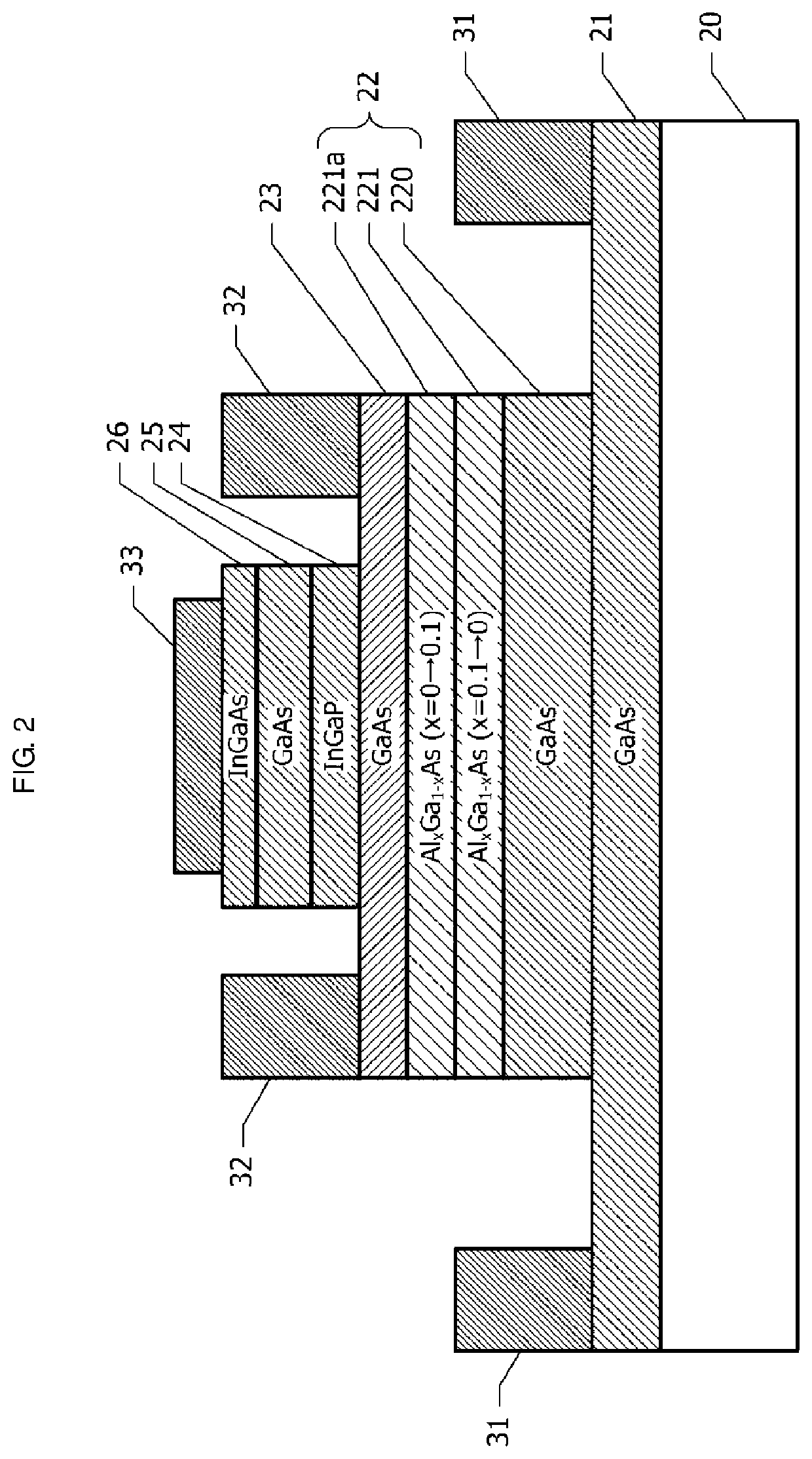
[0091]Next, modifications of the second embodiment will be described.

[0092]In the second embodiment, the AlAs mixed-crystal ratio x of the base layer 23 (FIG. 4) made of p-type AlxGa1-xAs is uniform with respect to the thickness direction. Alternatively, the AlAs mixed-crystal ratio x of the base layer 23 may be changed in the thickness direction. In such a case, the electron affinity is preferably gradually increased from the emitter layer 24 toward the collector layer 22. Preferably, for example, the AlAs mixed-crystal ratio x of the base layer 23 is linearly changed from 0.07 on the emitter layer 24 side to 0.05 on the collector layer 22 side. When the electron affinity has such a distribution, electrons can be drifted in the base layer 23. Consequently, the cutoff frequency ft can be improved.

[0093]In the second embodiment, the interface between a graded semiconductor layer made of AlGaAs and a uniform composition layer made of GaAs coincides wit...

third embodiment

[0099]Next, an HBT according to a third embodiment will be described with reference to FIG. 10. Hereinafter, descriptions of configurations that are common to those of the HBT (FIG. 4, etc.) according to the second embodiment will be omitted.

[0100]FIG. 10 is a sectional view of an HBT according to the third embodiment. In the third embodiment, an intermediate layer 27 made of a compound semiconductor that does not contain Al as a group III element is disposed between a collector layer 22 and a base layer 23. The intermediate layer 27 is made of, for example, n-type GaAs having a Si concentration of 3×1015 cm−3. The intermediate layer 27 has a thickness of, for example, 3 nm or more and 10 nm or less (i.e., from 3 nm to 10 nm).

[0101]In the third embodiment, after the collector layer 22 is epitaxially grown, the growth temperature is decreased while the intermediate layer 27 is grown. The base layer 23 is grown at a temperature lower than the growth temperature of the collector layer ...


PUM

PropertyMeasurementUnit
voltageaaaaaaaaaa
voltageaaaaaaaaaa
currentaaaaaaaaaa

Abstract

A heterojunction bipolar transistor includes a collector layer, a base layer, and an emitter layer that are stacked on a substrate. The collector layer includes a graded semiconductor layer in which an electron affinity increases from a side closer to the base layer toward a side farther from the base layer. An electron affinity of the base layer at an interface closer to the collector layer is equal to an electron affinity of the graded semiconductor layer at an interface closer to the base layer.

Description

CROSS-REFERENCE TO RELATED APPLICATION[0001]This application claims benefit of priority to Japanese Patent Application No. 2017-199029, filed Oct. 13, 2017, the entire content of which is incorporated herein by reference.BACKGROUNDTechnical Field[0002]The present disclosure relates to a heterojunction bipolar transistor.Background Art[0003]In mobile terminals, heterojunction bipolar transistors (HBTs) are mainly used as transistors included in power amplifier modules. Examples of characteristics required for HBTs include high efficiency, high gain, high output, high breakdown voltage, and low distortion in the radio-frequency range. In particular, recently, low distortion and high performance (high efficiency and high gain) have been desired for HBTs that are operated at high output.[0004]Japanese Unexamined Patent Application Publication No. 2000-332023 discloses an HBT aiming the achievement of high efficiency. The HBT includes an emitter layer, a base layer, a collector layer, an...

Claims


Application Information

Patent Timeline
Patent Type & Authority Patents(United States)
IPC IPC(8): H01L29/737H01L21/308H01L21/285H01L29/66H01L29/10H01L29/08H01L29/205H01L21/306H03F3/21
CPCH01L29/1004H01L29/205H01L29/0821H01L21/28575H01L29/66318H01L21/308H01L29/7371H01L21/30612H03F3/21H01L29/0817H01L29/0826H01L29/0684H01L29/201
Inventor UMEMOTO, YASUNARIKOYA, SHIGEKIOBU, ISAO
Owner MURATA MFG CO LTD
Why Eureka
Try Eureka