Plasma display device and method for manufacturing the same

a technology of plasma and display device, which is applied in the manufacture of electrode systems, instruments, electric discharge tubes/lamps, etc., can solve the problems of linearity decline, decrease of line-shaped electrode linearity, and decrease of lengthwise electrode linearity, so as to achieve effective suppression of edge curl

Inactive Publication Date: 2005-08-18
PANASONIC CORP
View PDF1 Cites 8 Cited by
  • Summary
  • Abstract
  • Description
  • Claims
  • Application Information

AI Technical Summary

Benefits of technology

[0029] In addition, in a case where electrodes are formed by a screen printing method in which the bus electrodes and the data electrodes are patterned by the and then baked, edge-curl does not occur too much in comparison with a photolithography method, because an amount of resin component in a paste for the screen printing and shrinkage percentage in baking are relatively small and therefore stress to camber upward is small. However, in the screen printing, linearity of the electrodes in a lengthwise direction decreases, because the paste flows due to steps such as leveling. Accordingly, when the electrodes are patterned by the screen printing method, a problem that the linearity of the line-shaped electrodes decreases occurs while edge-curl can be suppressed. According to the present invention as stated above, the linearity of the electrodes is maintained because the patterning is performed by exposure, and the surfaces of the side edges becomes rounded.
[0039] According to the conventional method, although the glass material becomes soft in baking, it does not become soft enough to touch the substrate by gravity, and therefore the stress is not resolved. According to the method of the present invention, however, baking is performed at a temperature such that the glass in the paste becomes soft so as to touch the substrate by gravity, and therefore the upward stress to cause edge-curl and camber the electrodes is resolved. In addition, the side edges becomes rounded by melted in baking, and the concentration of electric field is reduced in comparison with a case in which side edges are not round. Especially, the difference is remarkable when compared with a case in which the surface angle is sharp. As a result, the reliability of the panel improves, such as improvement in the isolation voltage.

Problems solved by technology

However, in the screen printing, linearity of the electrodes in a lengthwise direction decreases, because the paste flows due to steps such as leveling.
Accordingly, when the electrodes are patterned by the screen printing method, a problem that the linearity of the line-shaped electrodes decreases occurs while edge-curl can be suppressed.

Method used


Image

  • Plasma display device and method for manufacturing the same
  • Plasma display device and method for manufacturing the same
  • Plasma display device and method for manufacturing the same

Examples


first embodiment

[Construction of Panel]

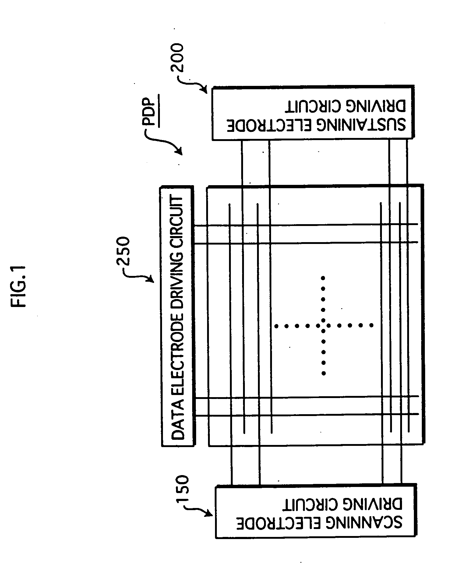
[0056]FIG. 1 is a block diagram illustrating a construction of an AC plasma display device according to the First Embodiment of the present invention.

[0057] As shown in this figure, an AC plasma display device comprises a plasma display panel and driving circuits 150, 200, and 250.

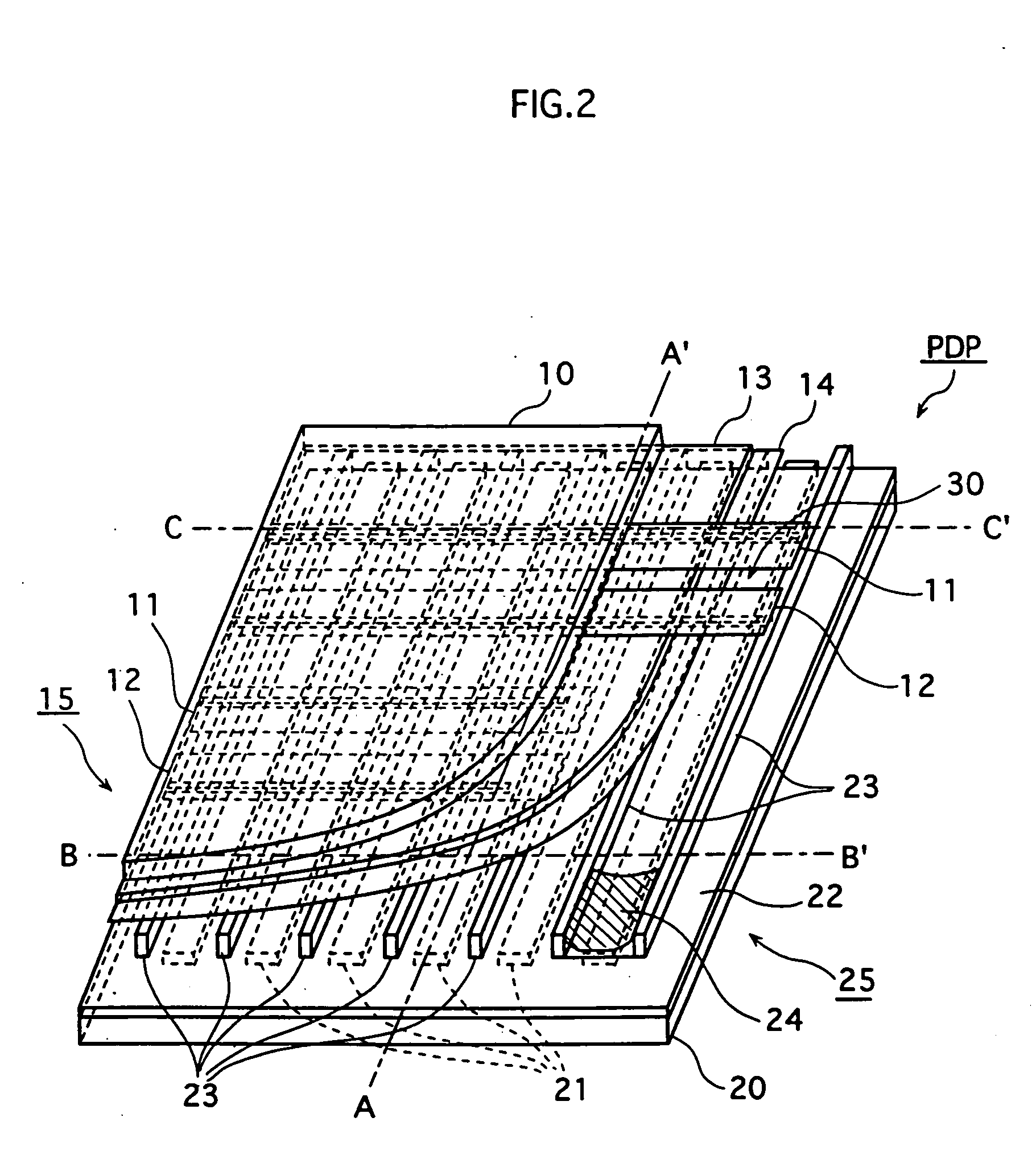
[0058]FIG. 2 is a perspective view illustrating a main construction of a PDP. As shown in this figure, the PDP comprises a front substrate 15 and a back substrate 25. The front substrate 15 is such that a plurality of pairs of line-shaped scanning electrodes 11 and sustaining electrodes 12 are disposed in parallel on a transparent first glass substrate 10, and a dielectric layer 13 and a protective layer 14 are laminated over the electrodes. The back substrate 25 is such that a plurality of line-shaped data electrodes 21, positioned perpendicular to the scanning electrodes 11 and the sustaining electrodes 12, are disposed on a second glass substrate 20, a dielectric layer 22 is di...

second embodiment

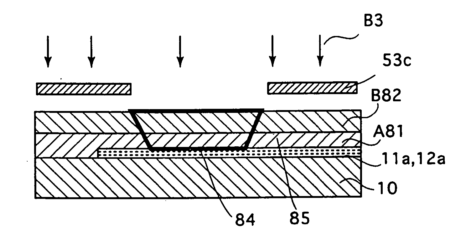
[0129] In the first embodiment, the widths of the exposure masks are set so that 53A (W1) becomes smaller than 53B (W2). According to the second embodiment, it is also possible to obtain the same effect in a case in which the upper layer is exposed using the same exposure mask used in the exposure of the upper layer, or using a exposure mask having the same width as the mask used in the exposure of the upper layer. Specifically, conditions are set as shown in the table 1, where at least one of the luminance, the light exposure, and the proxy amount (the distance between the mask and the substrate) is smaller than the conditions for the upper layer exposure. The rest of the process is conducted in the same manner as the first embodiment.

TABLE 1Examples of ExposureLightProxyWidth afterLuminanceExposureAmountDevelopment(mW / cm2)(mJ / cm2)(μm)(μm)Comparison1111ExampleExample 10.5110.9Example 210.1710.9Example 3110.50.9Example 40.50.1710.81Example 50.510.50.81Example 610.170.50.81Example ...

third embodiment

[0135] By a method for manufacturing the electrodes according to the third embodiment, like the first and second embodiments, it is possible to improve the production margin and to manufacture the electrodes having high reliability without disconnection by making the width of the lower layer smaller than the width of the upper layer. Specifically, the lower layer is exposed using an exposure mask, having smaller width than a mask used in the upper layer exposure, or the same exposure mask used in the exposure of the upper layer or a exposure mask having the same width as the mask used in the exposure of the upper layer under the similar conditions stated in the table 1, for example.

[0136] In the present embodiment, an example in which electrodes are formed into a shape having parts connecting two adjacent electrodes (hereinafter referred to as a short-bar) is explained. In a case in which fence electrodes made of a plurality of thin wires are used for the sustaining electrodes and ...


PUM

PropertyMeasurementUnit
softening pointaaaaaaaaaa
temperatureaaaaaaaaaa

Abstract

An object of the present invention is to provide a method for manufacturing electrodes that can effectively suppress edge-curl when metal electrodes such as bus electrodes and data electrodes are patterned mainly by a photolithography method. In order to achieve the above object, in the manufacturing method in the present invention, an amount of undercut generated by difference in a degree of dissolution caused by developing solution is controlled, and baking is performed at a temperature such that glass in a protrusion formed at side edges becomes soft so as to touch a substrate by gravity. With such method for manufacturing, it becomes possible to make the side edges rounded whose curvature changes continuously.

Description

TECHNICAL FIELD [0001] The present invention relates to plasma display devices and methods for manufacturing the same. More specifically, it relates to methods for forming electrodes that greatly contribute to improve reliability of the plasma display devices. BACKGROUND ART [0002] An example of conventional plasma display panels (hereinafter referred to as PDPs) is shown in FIG. 12, a perspective sectional view of a part of a conventional AC PDP. [0003] As shown in FIG. 12, the AC PDP comprises a front substrate 305 and a back substrate 315. The front substrate 305 is such that a plurality of pairs of line-shaped scanning electrodes 301 and sustaining electrodes 302 are disposed in parallel on a transparent first glass substrate 300 (insulating substrate), and a dielectric layer 303 and a protective layer 304 are laminated over the electrodes. The back substrate 315 is such that a plurality of line-shaped data electrodes 311, positioned perpendicular to the scanning electrodes 301 ...

Claims


Application Information

Patent Timeline
Patent Type & Authority Applications(United States)
IPC IPC(8): H01J9/02H01J11/12H01J11/22H01J11/24H01J17/04
CPCH01J9/02H01J11/12H01J2211/245H01J11/24H01J2211/225H01J11/22
Inventor ASHIDA, HIDEKIHIBINO, JUNICHISUMIDA, KEISUKEOHTANI, MITSUHIROFUJIWARA, SHINYAMARUNAKA, HIDEKINAKAGAWA, TADASHI
Owner PANASONIC CORP
Why Eureka
Try Eureka