Power amplification module

a power amplification and module technology, applied in amplifiers, amplifier types, amplifiers with semiconductor devices/discharge tubes, etc., can solve the problems of increasing current consumption, inability to control the gain reduction, and increasing current consumption, so as to suppress the degradation of the linearity of the gain of the power amplification module

Active Publication Date: 2016-11-03
MURATA MFG CO LTD
View PDF3 Cites 7 Cited by
  • Summary
  • Abstract
  • Description
  • Claims
  • Application Information

AI Technical Summary

Benefits of technology

[0009]According to the embodiment of the present disclosure, degradation of the linearity of gain in a power amplification module can be suppressed.

Problems solved by technology

A configuration has also been considered in which cutting of the negative part of the bias current is suppressed by increasing the amount of current that flows to the transistor Q2, but this configuration is not preferable since it results in an increase in current consumption.
Alternatively, cutting of the negative part of the bias current can also be suppressed by increasing the size of the current of the current source Ibias and increasing the size of the currents of the transistors Q2 and Q3, but there is a problem in that, in addition to the increase in current consumption, control to lower the gain cannot be performed.

Method used


Image

  • Power amplification module
  • Power amplification module
  • Power amplification module

Examples


Embodiment Construction

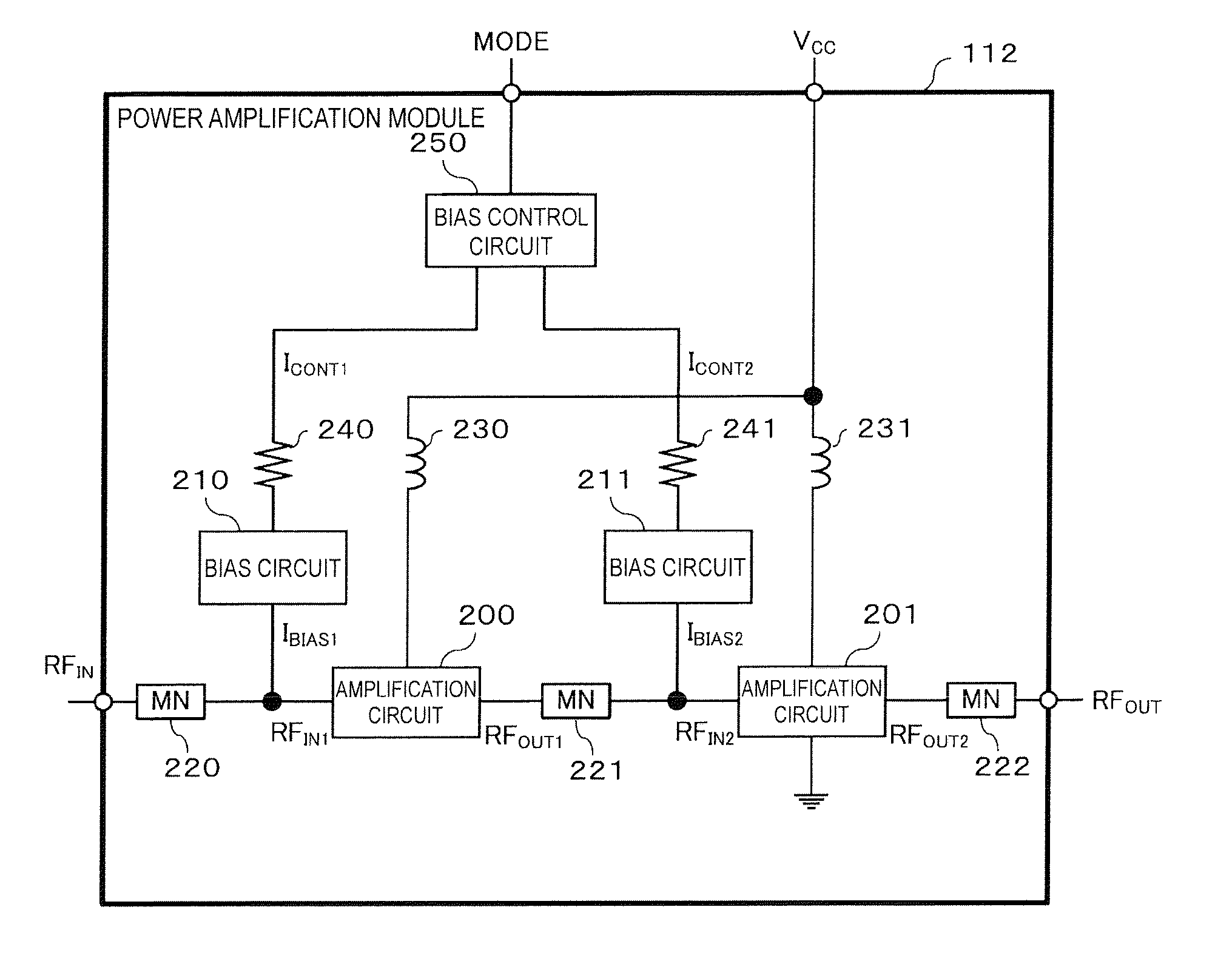
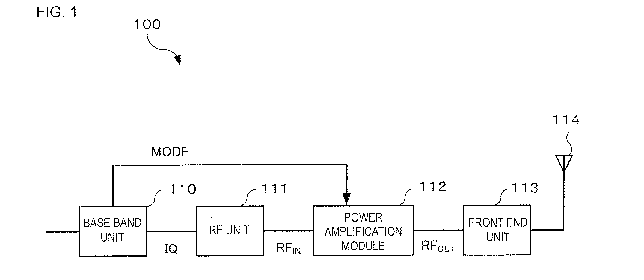
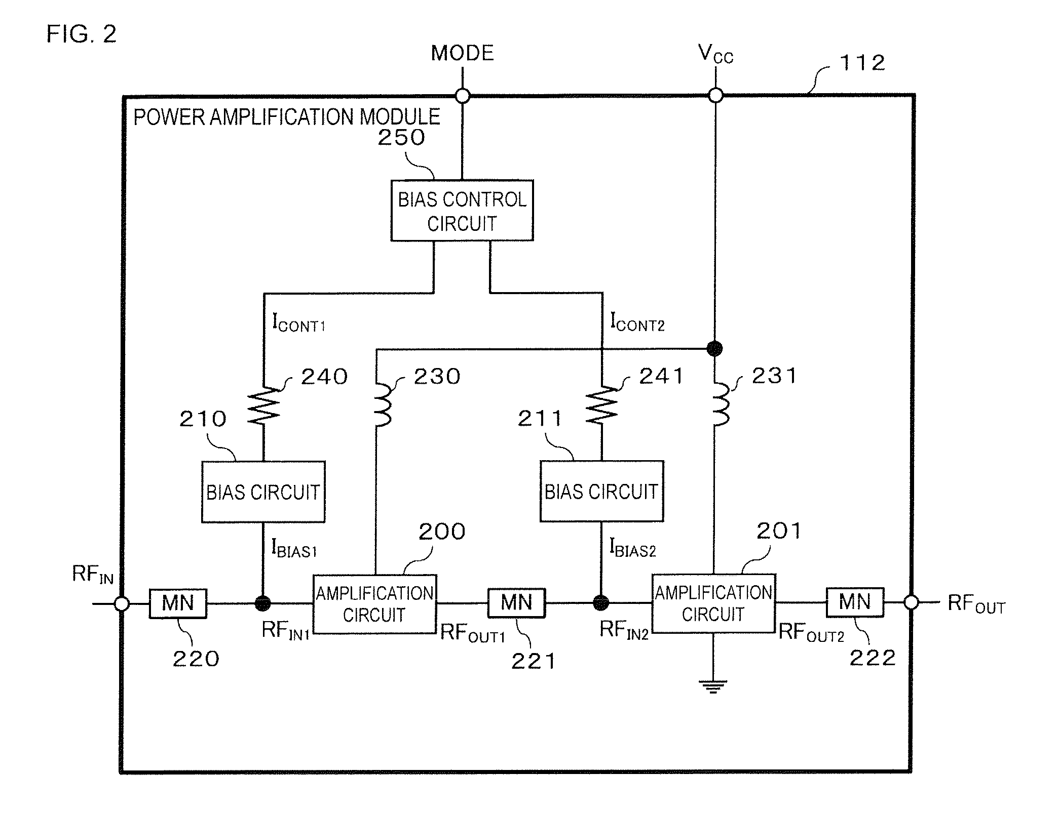
[0022]Hereafter, an embodiment of the present disclosure will be described while referring to the drawings. FIG. 1 illustrates an example configuration of a transmission unit that includes a power amplification module according to an embodiment of the present disclosure. A transmission unit 100 is for example used in a mobile communication device such as a cellular phone in order to transmit various signals such as speech and data to a base station. Although such a mobile communication device would also be equipped with a reception unit for receiving signals from the base station, the description of such a reception unit is omitted here.

[0023]As illustrated in FIG. 1, the transmission unit 100 includes a base band unit 110, an RF unit 111, a power amplification module 112, a front end unit 113 and an antenna 114.

[0024]The base band unit 110 modulates an input signal such as speech or data on the basis of a modulation scheme such as HSUPA or LTE and outputs a modulated signal. In thi...


PUM


Abstract

A power amplification module includes a first amplification transistor that receives a first signal outputs an amplified second signal from the collector thereof; and a bias circuit that supplies a bias current to the base of the first amplification transistor. The first bias circuit includes a first transistor that is diode connected and is supplied with a bias control current; a second transistor that is diode connected, the collector thereof being connected to the emitter of the first transistor; a third transistor, the base thereof being connected to the base of the first transistor, and the bias current being output from the emitter thereof; a fourth transistor, the collector thereof being connected to the emitter of the third transistor and the base thereof being connected to the base of the second transistor; and a first capacitor between the base and the emitter of the third transistor.

Description

BACKGROUNDTechnical Field[0001]The present disclosure relates to a power amplification module.[0002]A power amplification module is used in a mobile communication device such as a cellular phone in order to amplify the power of a radio frequency (RF) signal to be transmitted to a base station. A bias circuit is used in a power amplification module. The bias circuit is for supplying a bias current to a power amplification transistor. For example, in Japanese Unexamined Patent Application Publication (Translation of PCT Application) No. 2005-501458, there is disclosed a power amplification circuit that uses a bias circuit formed of a cascode current mirror circuit.[0003]FIG. 10 illustrates the configuration of the power amplification circuit disclosed in Japanese Unexamined Patent Application Publication (Translation of PCT Application) No. 2005-501458. In the power amplification circuit illustrated in FIG. 10, the bias circuit is formed of transistors Q2 to Q5 (cascode current mirror...

Claims


Application Information

Patent Timeline
Patent Type & Authority Applications(United States)
IPC IPC(8): H03F3/21H03F3/24H04B1/04H03F3/19
CPCH03F3/211H03F3/19H03F3/245H04B1/04H03F2203/21127H04B2001/0416H03F2203/21103H03F2200/318H03F2200/451H03F2200/411H03F2203/21139H03F1/3223H03F1/0261H03F3/191H03F2200/18H03F2200/222H03F2200/336H03F2200/387H03F2200/555H03F1/56H03F3/21
Inventor HASE, MASATOSHI
Owner MURATA MFG CO LTD
Why Eureka
Try Eureka