Vertical parasitic pnp device in a bicmos process and manufacturing method of the same

Active Publication Date: 2012-03-01
SHANGHAI HUAHONG GRACE SEMICON MFG CORP
View PDF2 Cites 1 Cited by
  • Summary
  • Abstract
  • Description
  • Claims
  • Application Information

AI Technical Summary

Benefits of technology

[0038]The vertical parasitic PNP transistor in a BiCMOS process in the present invention has a higher current amplification coefficient and better frequency characteristics. Therefore, the vertical parasitic PNP device can be used as output devices in high-speed and high-gain BiCMOS circuits to provide another choice of devices for the circuits. In the present invention, the collector of the transistor is picked up though the advanced deep-hole contact process to directly contact the P-t

Problems solved by technology

Its disadvantage is the large device area and the large connecting resistance of the collector.
Because the collector is picked up through another active region adjacent to the colle

Method used


Image

  • Vertical parasitic pnp device in a bicmos process and manufacturing method of the same
  • Vertical parasitic pnp device in a bicmos process and manufacturing method of the same
  • Vertical parasitic pnp device in a bicmos process and manufacturing method of the same

Examples


Example

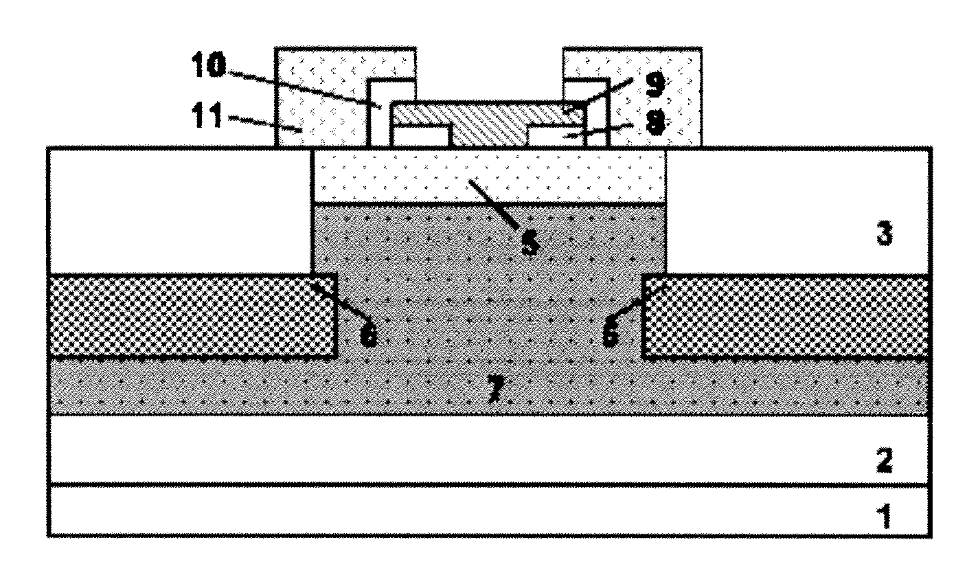
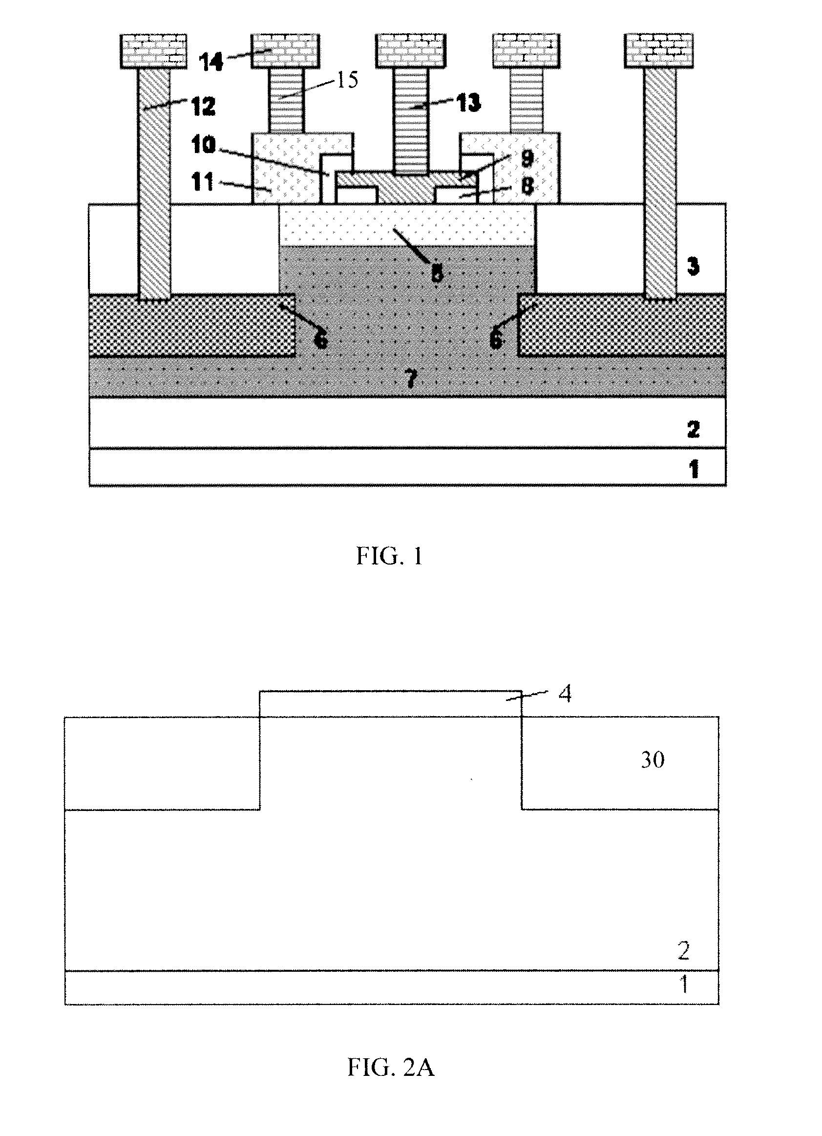
[0044]As shown in FIG. 1, which is a structural diagram of the vertical parasitic PNP transistor in a BiCMOS process in an embodiment of the present invention, the vertical parasitic PNP transistor is formed on a P-type silicon substrate 1 and an N-type deep well 2 is formed in the P-type silicon substrate 1. Active regions are isolated by shallow trench isolations (STIs) 3. The vertical parasitic PNP transistor includes:

[0045]A collector region 7, consisting of a P-type ion implantation region formed in the active region, which is deeper than or equal to the bottom of the STIs 3. The impurity implanted in the collector region 7 is boron and the P-type ion implantation can be realized through two steps of implantation: the dose for the implantation in step 1 is 1e11 cm−2˜5e13 cm−2, and the energy for the implantation is 100 keV˜300 keV; the dose for the implantation in step 2 is 5e11 cm−2˜1e13 cm−2, and the energy for the implantation is 30 keV˜100 keV.

[0046]Pseudo buried layers 6, ...


PUM


Abstract

The invention discloses a vertical parasitic PNP transistor in a BiCMOS process and manufacturing method of the same, wherein an active region is isolated by STIs. The transistor includes a collector region, a base region, an emitter region, pseudo buried layers, and N-type polysilicon. The pseudo buried layers, formed at the bottom of the STIs located on both sides of the collector region, extend laterally into the active region and contact with the collector region, whose electrodes are picked up through making deep-hole contacts in the STIs. The N-type polysilicon is formed on the base region and contacts with it, whose electrodes are picked up through making metal contacts on the N-type polysilicon. The transistors can be used as output devices in high-speed and high-gain circuits, efficiently reducing the transistors area, diminishing the collector resistance, and improving the transistors performance. The method can reduce the cost without additional technological conditions.

Description

CROSS-REFERENCE TO RELATED APPLICATIONS[0001]This application claims the priority of Chinese patent application number 201010270115.4, filed on Aug. 31, 2010, the entire contents of which are incorporated herein by reference.BACKGROUND OF THE INVENTION[0002]1. Field of the invention[0003]The present invention relates to the manufacturing field of semiconductor integrated circuits and, more particularly, to a vertical parasitic PNP transistor in a BiCMOS process. The present invention also relates to a manufacturing method of the vertical parasitic PNP transistor in a BiCMOS process.[0004]2. Description of Related Art[0005]Higher and higher cutoff frequency of devices is required for radio frequency (RF) applications. In BiCMOS processes, NPN transistors, particularly Silicon-Germanium heterojunction transistors (SiGe HBT), are good choice for ultra-high frequency devices. Besides, the SiGe process is basically compatible with the silicon process, therefore SiGe HBT has been one of t...

Claims


Application Information

Patent Timeline
IPC IPC(8): H01L21/331H01L29/732
CPCH01L21/76224H01L21/8249H01L29/0817H01L29/7371H01L29/41708H01L29/66242H01L29/161
Inventor QIAN, WENSHENGLIU, DONGHUAHUA, JUN
Owner SHANGHAI HUAHONG GRACE SEMICON MFG CORP
Why Eureka
Try Eureka