Semiconductor apparatus

Active Publication Date: 2013-03-14
RENESAS ELECTRONICS CORP
View PDF0 Cites 2 Cited by
  • Summary
  • Abstract
  • Description
  • Claims
  • Application Information

AI Technical Summary

Benefits of technology

[0010]The semiconductor apparatus according to the aspect of the present invention has the high-dielectric layer in a region including at least a position corresponding to the source-wire junction over the second surface of the lead frame. Thus, in the semiconductor apparatus according to the aspect of the present invention, a capacitor coupled in parallel to parasitic inductance components of the lead frame can be formed using this high-dielectric layer. By using the capacitor

Problems solved by technology

Unfortunately, the technologies using a series resonant circuit disclosed in Japanese Patent Nos. 3328542, 3612268, and 3825874 would degrade the stability of the amplifier circuit at frequencies other than the intended frequency, although they can reduce the impedance of the FET at a particular frequency.
For example, an amplifier circuit

Method used


Image

  • Semiconductor apparatus
  • Semiconductor apparatus
  • Semiconductor apparatus

Examples


Example

[0036]As shown in FIG. 1, the semiconductor apparatus 1 according to the first embodiment includes a semiconductor chip 10, bonding wires 11, a lead frame, a resin mold 15, and high-dielectric layers 16. The semiconductor apparatus 1 according to the first embodiment also includes a cap (not shown in FIG. 1). In FIG. 1, the lead frame which is covered by the resin mold 15 and thus cannot be recognized visually is represented by a broken line.

[0037]The lead frame includes a source electrode lead 12, a drain electrode lead 13, and a gate electrode lead 14. The semiconductor chip 10 is disposed over the source electrode lead. The semiconductor apparatus 1 according to the first embodiment has a GaAsFET formed over the semiconductor chip 10. The source of this GaAsFET is coupled to the source electrode lead 12, the drain thereof to the drain electrode lead 13, and the gate thereof to the gate electrode lead 14 via the corresponding bonding wires 11, respectively.

[0038]In the semiconduct...

Example

Second Embodiment

[0073]In a second embodiment, a plate equivalent to the first source wiring 20 formed over the substrate 23 according to the first embodiment is disposed in a semiconductor apparatus. FIG. 15 is a bottom view of a semiconductor apparatus 2 according to a second embodiment. The top view of the semiconductor apparatus 2 is the same as the semiconductor apparatus 1 according to the first embodiment and therefore will not be described. As shown in FIG. 15, the semiconductor apparatus 2 according to the second embodiment includes an additional source electrode plate 50 that couples one end and the other end of the source electrode lead 12.

[0074]FIG. 16 is a sectional view of the semiconductor apparatus 2 taken along line XVI-XVI of FIG. 15. As shown in FIG. 16, the additional source electrode plate 50 is formed so as to couple one end and the other end of the source electrode lead 12 and the bottom surface of the resin mold 15. FIG. 17 is a sectional view of the semicond...

Example

Third Embodiment

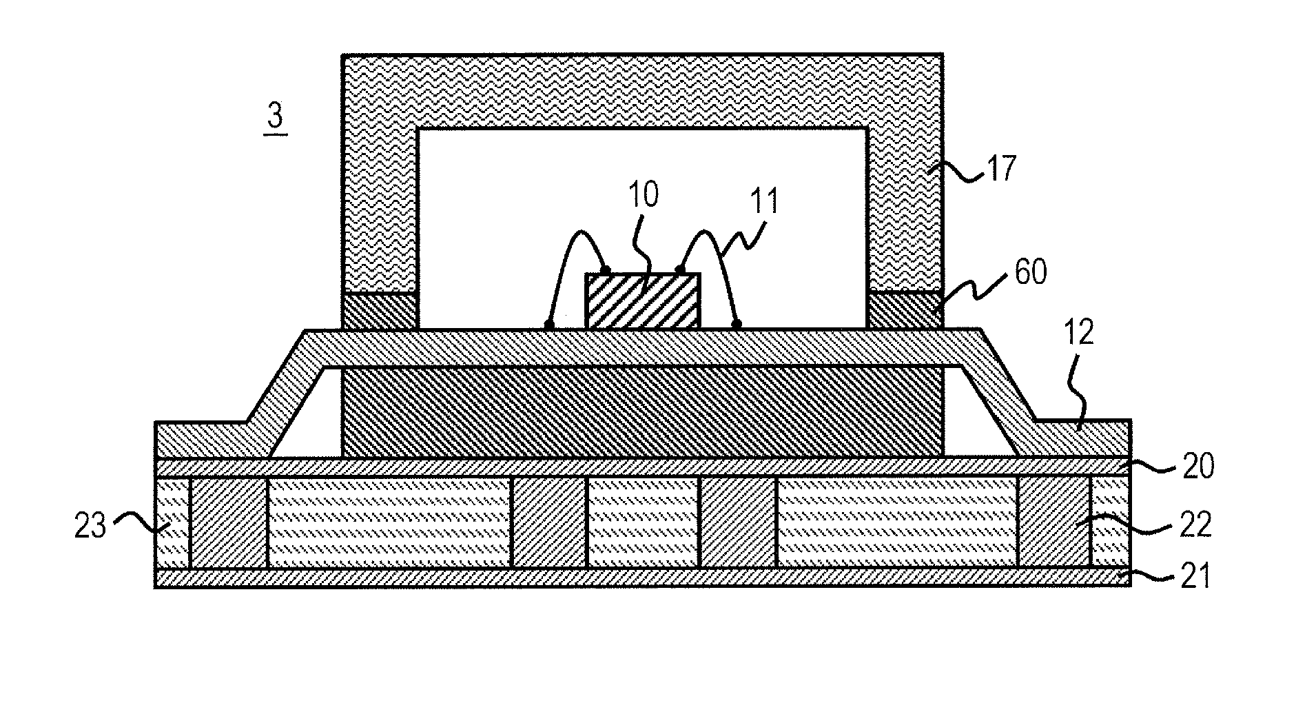
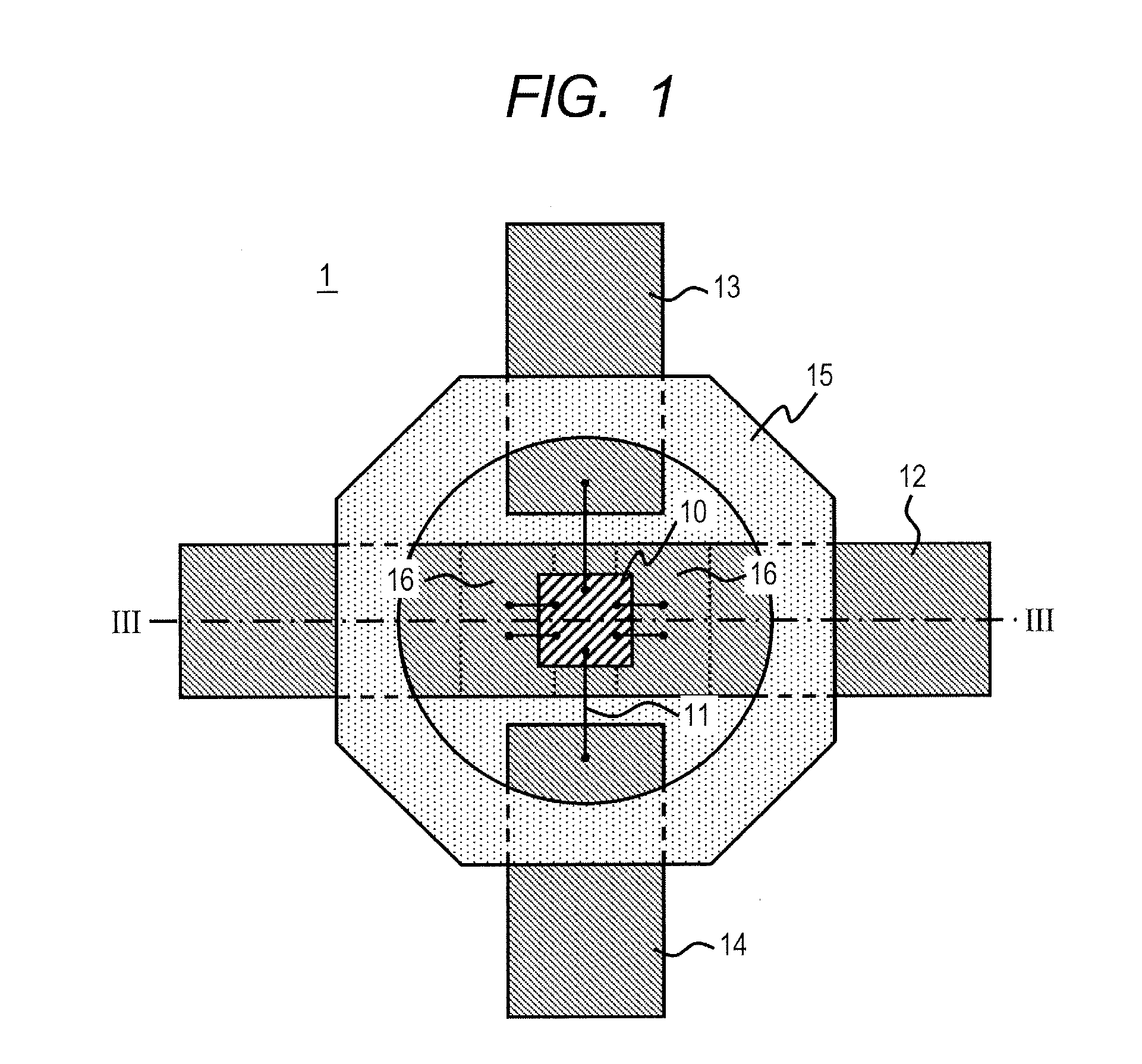
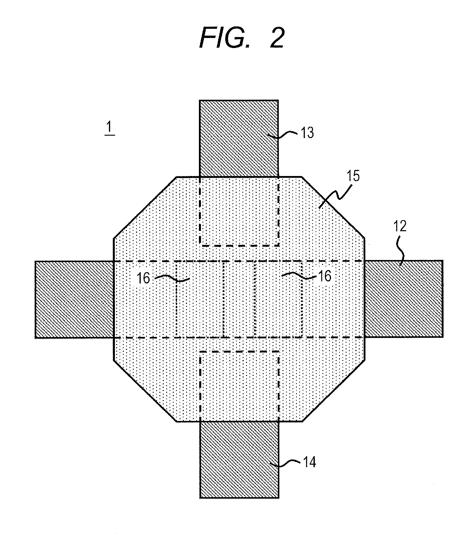
[0078]In a third embodiment, a resin mold is formed as a high-dielectric layer rather than using a dielectric chip. FIG. 19 shows a top view of a semiconductor apparatus 3 according to a third embodiment. As shown in FIG. 19, the semiconductor apparatus 3 according to the third embodiment has the same shape as the semiconductor apparatus 1 according to the first embodiment. However, the semiconductor apparatus 3 includes a resin mold 60 rather than the resin mold 15 of the semiconductor apparatus 1 according to the first embodiment.

[0079]FIG. 20 is a bottom view of the semiconductor apparatus 3 according to the third embodiment. As shown in FIG. 20, the semiconductor apparatus 3 according to the third embodiment has the same shape as the semiconductor apparatus 1 according to the first embodiment. However, the semiconductor apparatus 3 includes the resin mold 60 rather than the resin mold 15 of the semiconductor apparatus 1 according to the first embodiment.

[0080]FIG...


PUM


Abstract

A semiconductor apparatus includes a semiconductor chip, a lead frame that has a first surface having the semiconductor chip mounted thereover and a second surface opposite to the first surface, a bonding wire that couples the semiconductor chip and the lead frame, and a high-dielectric layer that is disposed over a surface of the lead frame opposite to a surface having the semiconductor chip mounted thereover and that has a relative permittivity of 5 or more. The lead frame includes a source electrode lead coupled to the source of a semiconductor device formed over the semiconductor chip and a source-wire junction at which the source electrode lead and the bonding wire are coupled together. The high-dielectric layer is disposed in a region including at least a position corresponding to the source-wire junction over the second surface of the lead frame.

Description

CROSS-REFERENCE TO RELATED APPLICATIONS[0001]The disclosure of Japanese Patent Application No. 2011-196644 filed on Sep. 9, 2011 including the specification, drawings, and abstract is incorporated herein by reference in its entirety.BACKGROUND[0002]The present invention relates to a semiconductor apparatus and in particular to a semiconductor apparatus including a semiconductor chip over which an amplifier circuit for amplifying high-frequency signals is formed.[0003]Radio signal systems include an amplifier circuit for handling high-frequency signals in a microwave band. Among examples of such an amplifier circuit is a field-effect transistor (FET) including a GaAs substrate. Such an FET including a GaAs substrate will be referred to as a GaAsFET. A semiconductor apparatus that handles such high-frequency signals requires a technology that reduces a parasitic capacitance related to a semiconductor chip to improve high-frequency characteristics. Technologies for reducing a parasitic...

Claims


Application Information

Patent Timeline
IPC IPC(8): H01L23/48
CPCH01L2924/16152H01L2224/49175H05K1/0243H01L2224/49111H01L23/642H01L23/047H01L24/48H01L2924/00014H05K1/113H01L2224/48247H05K1/114H01L2924/3011H01L2224/48257H01L2223/6655H01L2924/30107H01L24/49H01L23/49861H01L23/66H05K1/025H01L2924/00H01L2224/45099
Inventor SAKURA, NAOKI
Owner RENESAS ELECTRONICS CORP
Why Eureka
Try Eureka