Parasitic Vertical PNP Bipolar Transistor And Its Fabrication Method In Bicmos Process

Active Publication Date: 2011-06-30
SHANGHAI HUAHONG GRACE SEMICON MFG CORP
View PDF2 Cites 7 Cited by
  • Summary
  • Abstract
  • Description
  • Claims
  • Application Information

AI Technical Summary

Benefits of technology

[0004]This invention provides a parasitic vertical PNP bipolar transistor in the BiCMOS (Bipolar Complementary Metal Oxide Semiconductor) process which can be used as the high speed, high current and power gain IO (Input / Output) device and a device option for circuit design. This invention also provides the fabrication method of this parasitic vertical PNP bipolar transistor which without additional process and additional cost.
[0015]This parasitic vertical PNP bipolar transistor has a current gain high than 15 and good frequency characteristics. The transistor can be used as the high speed and high current & power current IO device and one more choice for circuit design. The fabrication method of this parasitic transistor adapts the existing Pwell implanting, NLDD (N-type Lightly Doped Drain) implanting, base eptaxy layer of NPN bipolar transistor in BiCMOS (Bipolar Complementary Metal Oxide Semiconductor) process without additional process and cost. This invention also avoids use the buried layer, collector epitaxy and deep trench isolation process and drive the cost low more.

Problems solved by technology

This process needs high temperature and long time furnace drive-in to make the dopant to diffuse deeper and decrease the capacitance between buried layer and silicon substrate.
The existing parasitic PNP bipolar transistor design in BiCMOS (Bipolar Complementary Metal Oxide Semiconductor) process has the very mature and reliable process, but also comes with the disadvantages as below: 1. buried layer needs high temperature and long time furnace drive-in; 2. high cost of collector epitaxy; 3. process complication and high cost of deep trench isolation.

Method used


Image

  • Parasitic Vertical PNP Bipolar Transistor And Its Fabrication Method In Bicmos Process
  • Parasitic Vertical PNP Bipolar Transistor And Its Fabrication Method In Bicmos Process
  • Parasitic Vertical PNP Bipolar Transistor And Its Fabrication Method In Bicmos Process

Examples


Embodiment Construction

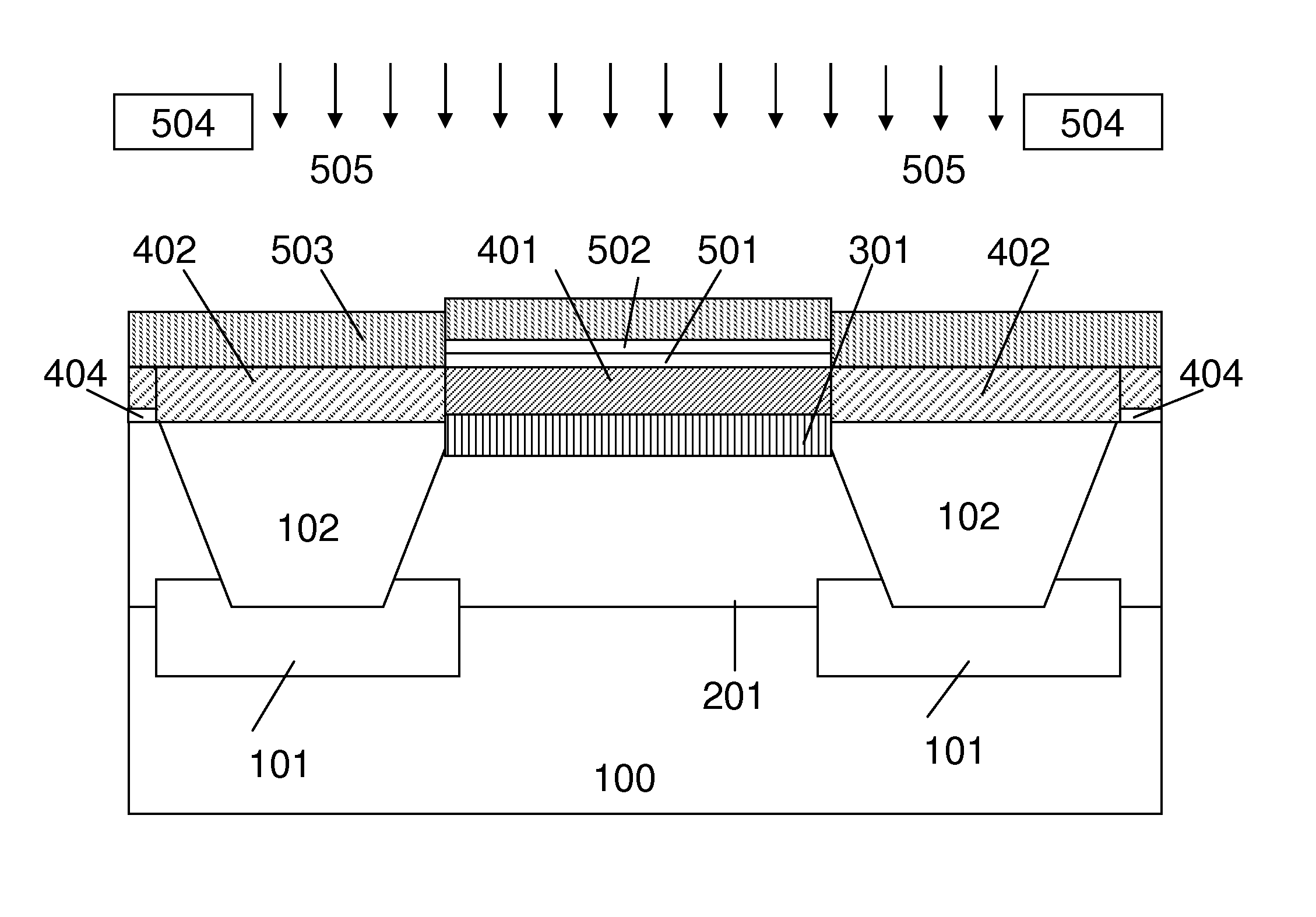
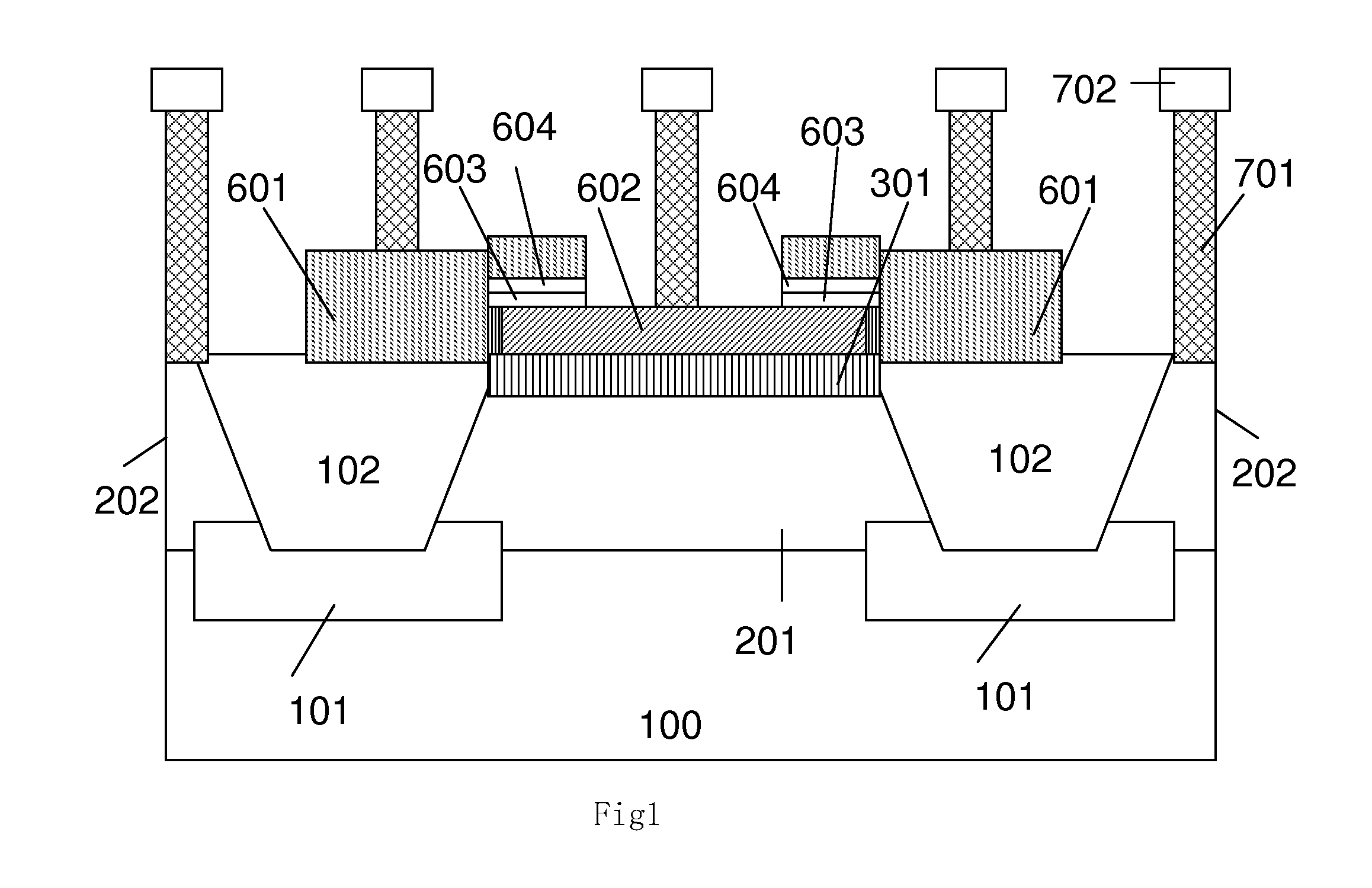
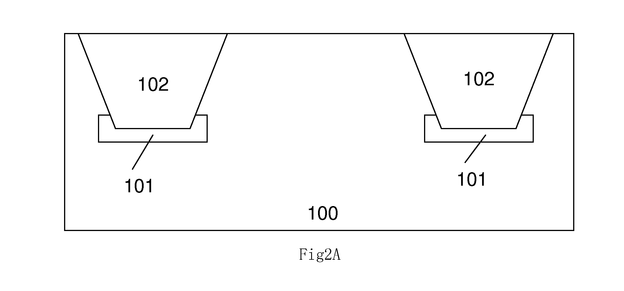
[0021]FIG. 1 illustrates the parasitic vertical PNP in BiCMOS (Bipolar Complementary Metal Oxide Semiconductor) process of this invention. The active region is isolated by STI field oxide which is the STI 102 on silicon substrate 100 as showed in FIG. 1. The PNP bipolar transistor structure comprises a collector 201, a base 301 and an emitter 602.

[0022]The collector 201 is formed by the p-type ion implanting layer in the first active region. This p-type implantation shares the Pwell implant of MOSFET of the BiCMOS process. The Pwell implantation has three steps: the first step, implanting species is boron, dose range from 1e12˜5e13 cm-2 and energy range from 200˜300 keV; the second step, implanting species is boron, dose range from 5e11˜1e13 cm-2 and energy range from 25˜200 keV; the third step, implanting species is boron, dose range from 1e11˜1e13 cm-2 and energy range from 5˜25 keV. Or only use the condition of the second and the third step to form the p-type collector layer. Thi...


PUM


Abstract

This invention published a parasitic vertical PNP bipolar transistor in BiCMOS (Bipolar Complementary Metal Oxide Semiconductor) process; the bipolar transistor comprises a collector, a base and an emitter. Collector is formed by active region with p-type ion implanting layer. It connects a p-type buried layer which formed in the bottom region of STI (Shallow Trench Isolation). The collector terminal connection is through the p-type buried layer and the adjacent active region. The base is formed by active region with n type ion implanting which is on the collector. Its connection is through the original p-type epitaxy layer after converting to n-type. The emitter is formed by the p-type epitaxy layer on the base region with heavy p-type doped. This invention also comprises the fabrication method of this parasitic vertical PNP bipolar in BiCMOS (Bipolar Complementary Metal Oxide Semiconductor) process. And this PNP bipolar transistor can be used as the IO (Input / Output) device in high speed, high current and power gain BiCMOS (Bipolar Complementary Metal Oxide Semiconductor) circuits. It also provides a device option with low cost.

Description

[0001]The current application claims a foreign priority to the application China 200910202031.4 filed on Dec. 24, 2009.FIELD OF THE INVENTION[0002]This invention relates generally to semiconductor devices in integrated circuits. More particularly it relates to bipolar transistor design and fabrication.BACKGROUND OF THE INVENTION[0003]Currently the NPN bipolar transistor in BiCMOS (Bipolar Complementary Metal Oxide Semiconductor) process usually use heavy doped collector buried layer to reduce the collector resistance. This process needs high temperature and long time furnace drive-in to make the dopant to diffuse deeper and decrease the capacitance between buried layer and silicon substrate. This process also need n-type heavy implanting (above 1e15 cm-2) to realize n-type buried layer connection and form collector pick-up. The epitaxy layer on the collector buried layer forms the collector. The p-type doped Silicon or SiGe (Silicon Germanium) epitaxy forms the base and the heavy do...

Claims


Application Information

Patent Timeline
IPC IPC(8): H01L27/07H01L21/8249
CPCH01L21/8249H01L27/0623H01L29/0821H01L29/7371H01L29/66242H01L29/66287H01L29/732H01L29/1004
Inventor CHIU, TZUYINCHU, TUNGYUANQIAN, WENSHENGFAN, YUNGCHIEHLIU, DONGHUAHU, JUN
Owner SHANGHAI HUAHONG GRACE SEMICON MFG CORP
Why Eureka
Try Eureka