Semiconductor device with air gap and method for fabricating the same

a technology of semiconductor devices and air gaps, which is applied in the direction of semiconductor devices, semiconductor/solid-state device details, electrical apparatus, etc., can solve the problems of reducing the size of semiconductor device products, limiting the distance between conductive layer patterns, and slow operation speed of dynamic random access memory devices including bit lines laid adjacent to storage nodes contact plugs. , to achieve the effect of reducing parasitic capacitan

Active Publication Date: 2013-12-05
SK HYNIX INC
View PDF0 Cites 112 Cited by
  • Summary
  • Abstract
  • Description
  • Claims
  • Application Information

AI Technical Summary

Benefits of technology

[0010]An embodiment of the present invention is directed to a semiconductor device having a decreased parasitic capacitance between a bit line and a storage node contact plug, and a method for fabricating the semiconductor device.

Problems solved by technology

In particular, a Dynamic Random Access Memory (DRAM) device including bit lines laid adjacent to storage node contact plugs may have a slow operation speed and a deteriorated refresh characteristic because of the increase in the parasitic capacitance between the bit line and the storage node contact plug.
However, there is limitation in increasing the distance between the conductive layer patterns because the size of semiconductor device products is decreased.
Since the silicon oxide layer and the silicon nitride layer still have high dielectric constants, there may be limitation in decreasing the parasitic capacitance.
Recently, some layers having relatively low dielectric constants, such as silicon boron nitride (SiBN) and silicon carbon nitride (SiCN), are under development, but their dielectric constants approach approximately 6, which may be not sufficiently low.

Method used


Image

  • Semiconductor device with air gap and method for fabricating the same
  • Semiconductor device with air gap and method for fabricating the same
  • Semiconductor device with air gap and method for fabricating the same

Examples


Embodiment Construction

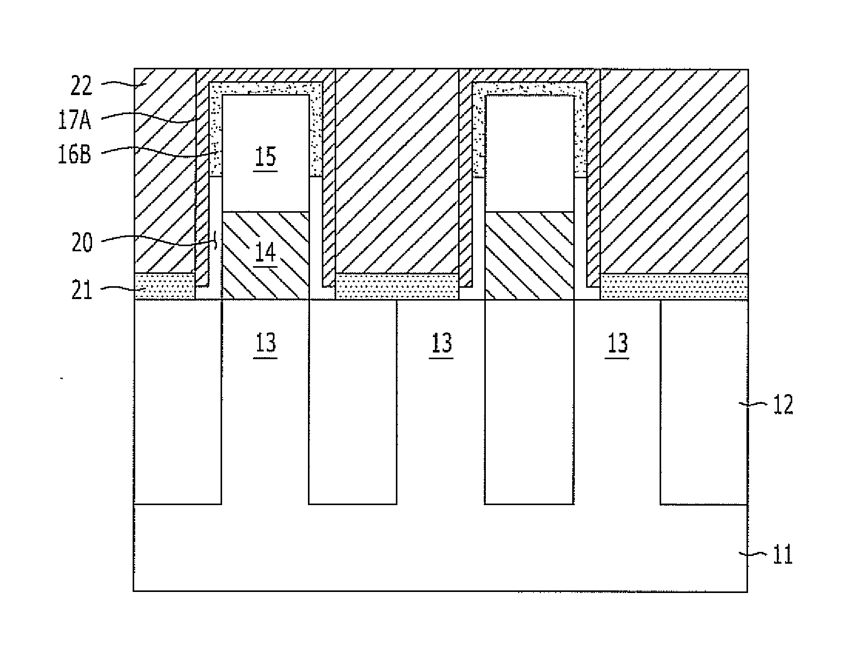
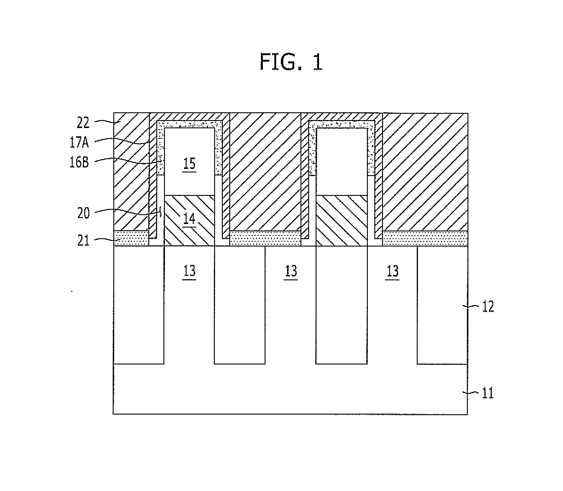
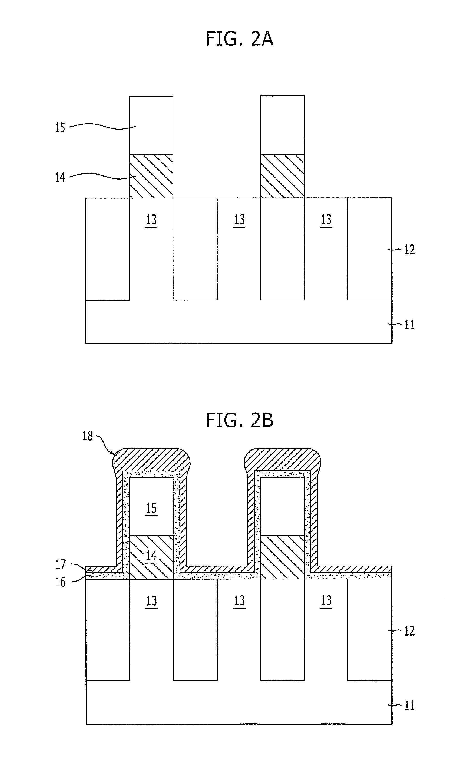
[0030]Exemplary embodiments of the present invention will be described below in more detail with reference to the accompanying drawings. The present invention may, however, be embodied in different forms and should not be construed as limited to the embodiments set forth herein. Rather, these embodiments are provided so that this disclosure will be thorough and complete, and will fully convey the scope of the present invention to those skilled in the art. Throughout the disclosure, like reference numerals refer to like parts throughout the various figures and embodiments of the present invention.

[0031]The drawings are not necessarily to scale and in some instances, proportions may have been exaggerated in order to clearly illustrate features of the embodiments. When a first layer is referred to as being “on” a second layer or “on” a substrate, it not only refers to a case where the first layer is formed directly on the second layer or the substrate but also a case where a third laye...


PUM


Abstract

A method for fabricating a semiconductor device includes forming a plurality of bit line structures over a substrate, forming multiple layers of spacer layers with a capping layer interposed therebetween over the bit line structures, exposing a surface of the substrate by selectively etching the spacer layers, forming air gaps and capping spacers for covering upper portions of the air gaps by selectively etching the capping layer, and forming storage node contact plugs between the bit line structures.

Description

CROSS-REFERENCE TO RELATED APPLICATIONS[0001]The present application claims priority of Korean Patent Application No. 10-2012-0058435, filed on May 31, 2012, which is incorporated herein by reference in its entirety.BACKGROUND[0002]1. Field[0003]Exemplary embodiments of the present invention relate to a semiconductor device, and more particularly, to a semiconductor device with air gaps and a method for fabricating the semiconductor device.[0004]2. Description of the Related Art[0005]Generally, a semiconductor device includes a plurality of first conductive layer patterns and a plurality of second conductive layer patterns. Each second conductive layer pattern is formed between the first conductive layer patterns, but an insulation is between the first conductive layer pattern and the second conductive layer pattern. The first conductive layer patterns may include a gate electrode, bit lines, and metal lines. The second conductive layer patterns may include contact plugs, storage no...

Claims


Application Information

Patent Timeline
Patent Type & Authority Applications(United States)
IPC IPC(8): H01L21/768H01L23/48
CPCH01L21/7682H01L21/76897H01L21/76832H01L21/76834H01L21/76885H10B12/482H01L21/3205
Inventor KIM, JUN KI
Owner SK HYNIX INC
Why Eureka
Try Eureka