

Display device
a technology of display device and display portion, which is applied in the direction of static indicating device, instruments, optics, etc., can solve the problems of product defect and luminance decrease, and achieve the effect of preventing the separation of thin films, increasing the thickness of the pad portion, and reducing the resistance of thin film separation
- Summary
- Abstract
- Description
- Claims
- Application Information
AI Technical Summary
Benefits of technology
Problems solved by technology
Method used
Image

Examples
embodiment 1
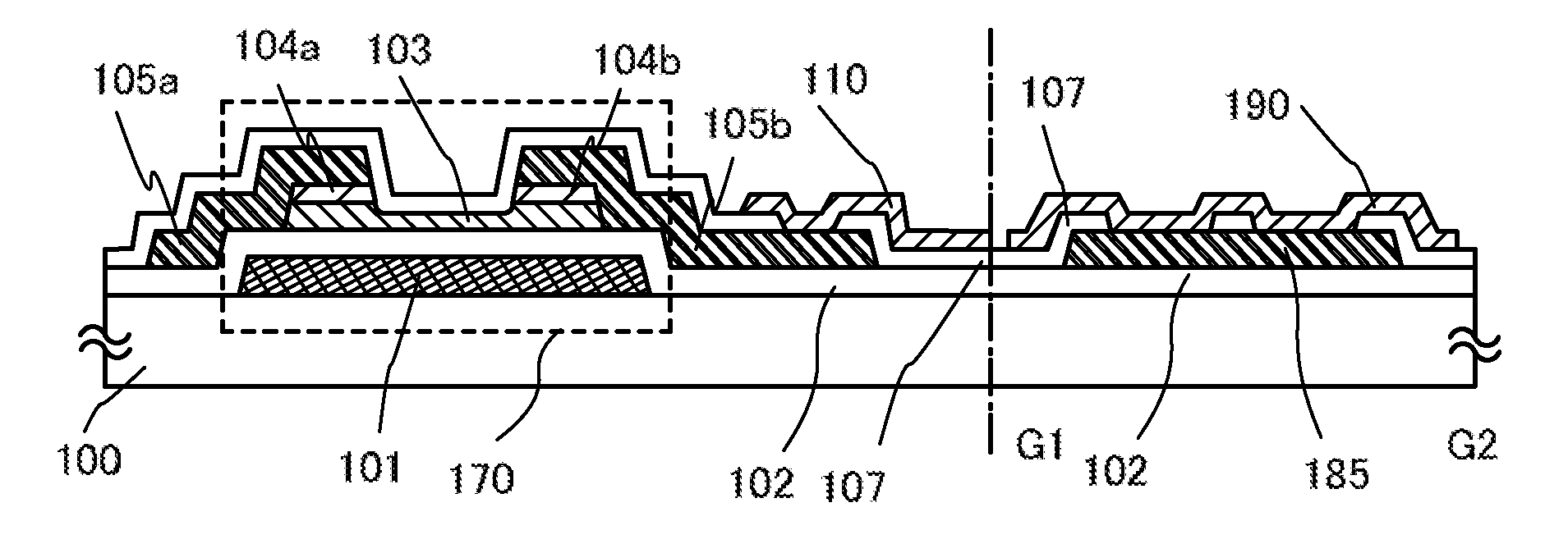
[0082]This embodiment shows an example of a liquid crystal display device in which a liquid crystal layer is sealed between a first substrate and a second substrate, and a common connection portion (a pad portion) is formed over the first substrate to be electrically connected to a counter electrode provided on the second substrate. Note that a thin film transistor is formed as a switching element over the first substrate, and the common connection portion is manufactured in the same process as the switching element in a pixel portion, resulting in simplified process.
[0083]The common connection portion is provided in a position overlapping a sealant for bonding the first substrate and the second substrate and is electrically connected to a counter electrode through conductive particles in the sealant. Alternatively, the common connection portion is provided in a position which does not overlap the sealant (except for the pixel portion) and a paste including conductive particles is p...
embodiment 2
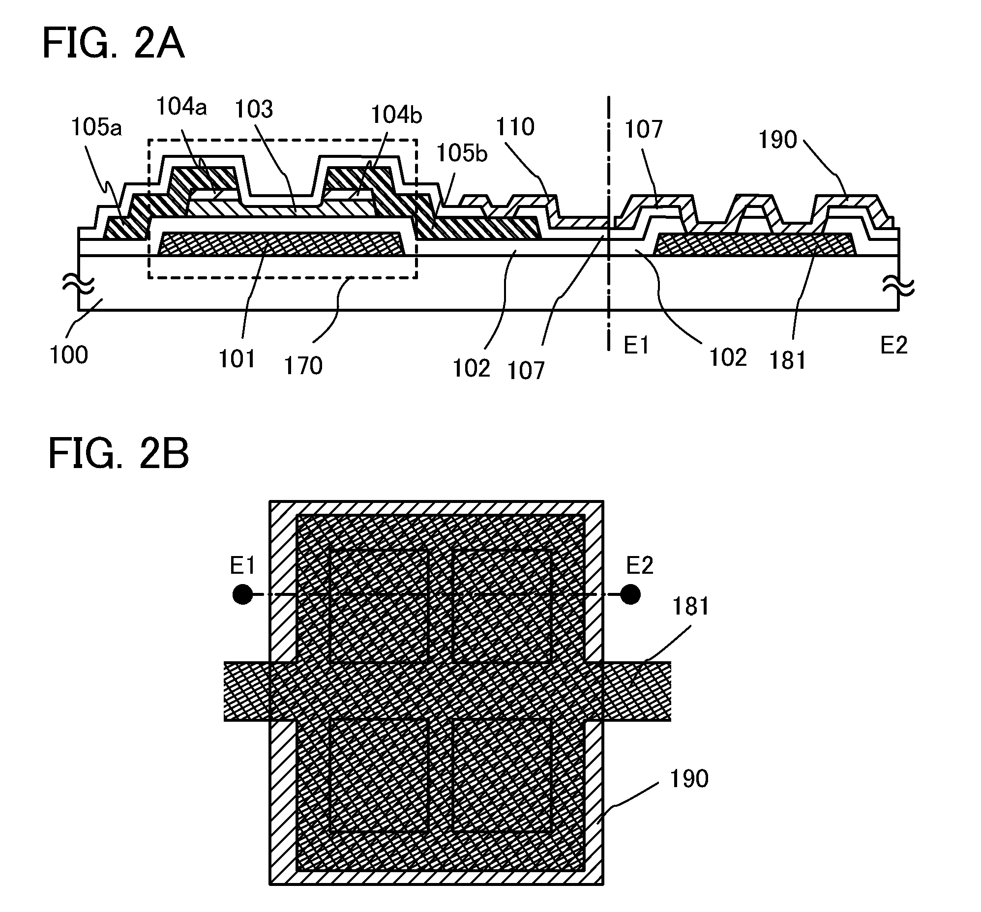
[0098]In this embodiment, an example of manufacturing a common connection portion (a pad portion), in which a wiring formed of the same material and in the same process as a gate wiring is used as a common potential line, will be illustrated in FIGS. 2A and 2B.
[0099]FIG. 2B illustrates an example of a top view of a common connection portion, and dashed line E1-E2 in FIG. 2B corresponds to a cross section of the common connection portion of FIG. 2A.
[0100]Note that as illustrated in FIG. 2A, a thin film transistor in a pixel portion has the same structure as that of Embodiment 1; thus, portions similar to those in FIG. 1A are denoted by the same reference numerals and detailed description is omitted here.
[0101]A common potential line 181 is provided over the substrate 100 and manufactured of the same material and in the same process as a gate electrode layer 101.
[0102]In addition, the common potential line 181 is covered with the gate insulating layer 102 and the protective insulating...
embodiment 3
[0110]In this embodiment, an example of manufacturing a common connection portion (a pad portion), in which an electrode formed of the same material and in the same process as a gate wiring is formed and a wiring formed of the same material and in the same process as a source electrode layer is provided as a common potential line over the electrode, will be illustrated in FIGS. 3A and 3B.
[0111]FIG. 3B illustrates an example of a top view of a common connection portion, and dashed line F1-F2 in FIG. 3B corresponds to a cross section of the common connection portion of FIG. 3A.
[0112]Note that as illustrated in FIG. 3A, a thin film transistor in a pixel portion has the same structure as that of Embodiment 1; thus, portions similar to those in FIG. 1A are denoted by the same reference numerals and detailed description is omitted here.
[0113]A connection electrode layer 191 is provided over the substrate 100 and manufactured of the same material and in the same process as the gate electro...
PUM
 Abstract
Description
Claims
Application Information