Semiconductor memory device

Active Publication Date: 2005-07-26
SOCIONEXT INC
View PDF7 Cites 123 Cited by
  • Summary
  • Abstract
  • Description
  • Claims
  • Application Information

AI Technical Summary

Benefits of technology

[0054]According to this configuration, an advantage of the first semiconductor memory device that there are few probability of a short circuit failure between the bit line and the VSS power supply is used effectively, only the row r

Problems solved by technology

However, since many interconnection patterns exist in the second-layer interconnection, a capacitance difference to the substrate is hardly effective.
Further, as can be seen when comparing FIG. 25 with FIG. 27, since the number of signals transmitted from the lower layer to the upper layer of the third layer bit line type are larger than that of the second layer bit line type, the number of via sections to be used increases, and thereby it may become disadvantageous in yield.
However, there exists a problem also in the horizontal memory cell.
Although r

Method used


Image

  • Semiconductor memory device
  • Semiconductor memory device
  • Semiconductor memory device

Examples


first embodiment

[0084]A first embodiment will be described using the drawings. A semiconductor memory device according to this embodiment represents a CMOS SRAM comprising a horizontal memory cell of a second layer bit line type.

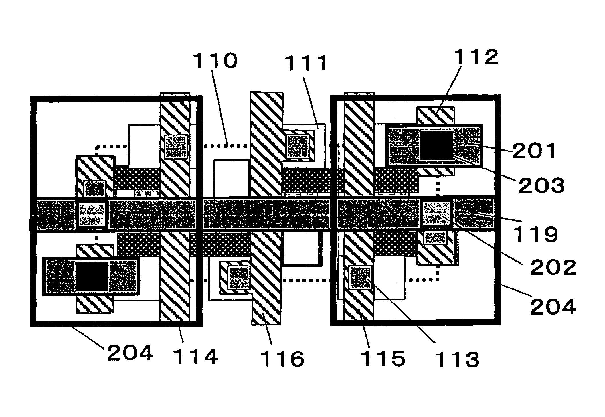
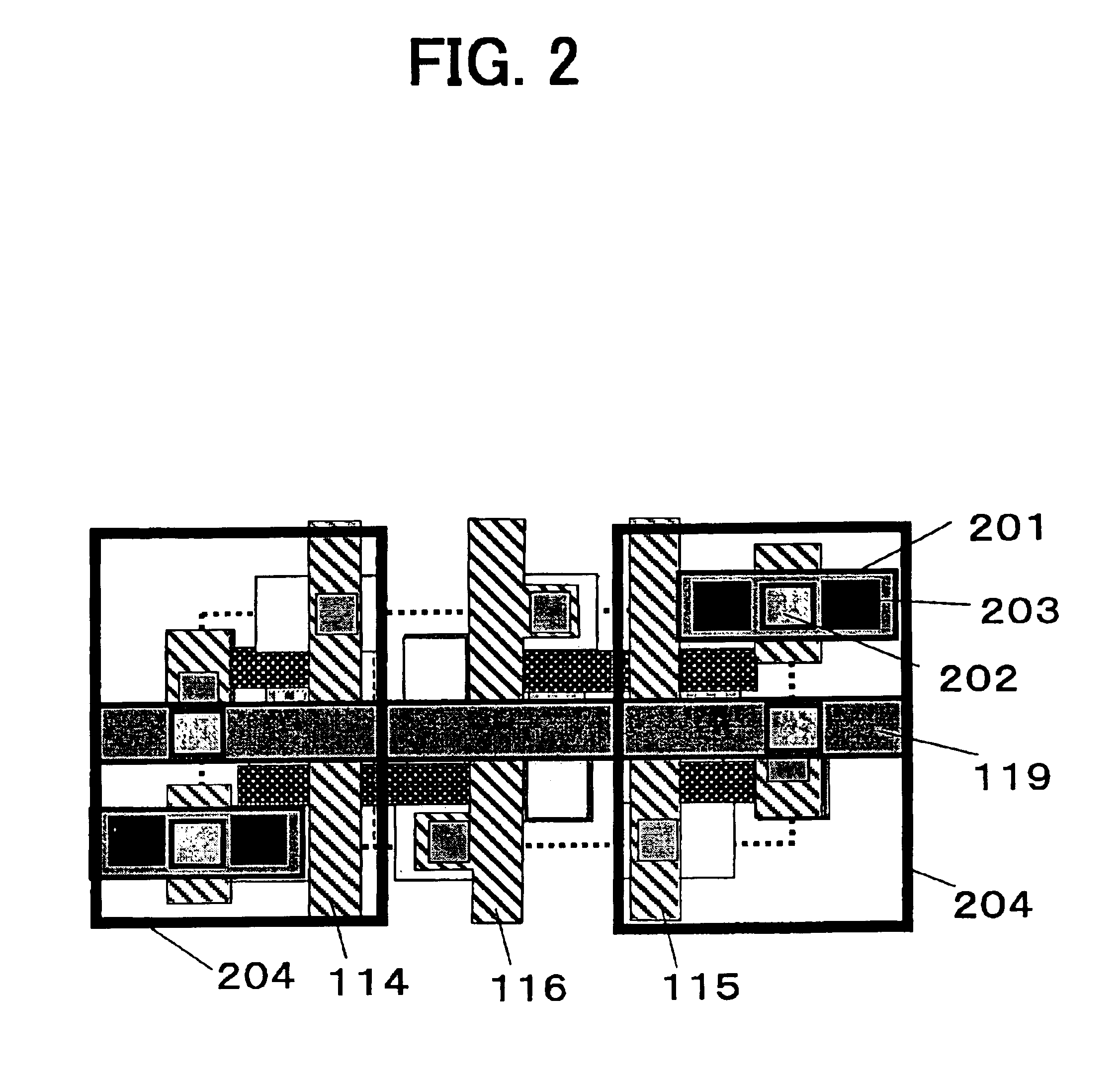
[0085]A layout of a lower layer section of the horizontal memory cell in this embodiment, and a layout of a first-layer interconnection and a second-layer interconnection upper than that are similar to those of conventional examples of FIGS. 21 to 24; and further an arrangement of the memory cell is also arranged in flip as shown in FIG. 22, and a circuit diagram of the memory cell is shown in FIG. 28. An example of an interconnection layout according to this embodiment is shown in FIG. 1. In FIG. 1, reference numerals 201, 202, 203, and 204 represent a VSS node with an island-shaped pattern formed with a third-layer interconnection, a via section of connecting the second-layer interconnection to the third-layer interconnection, a via section of connecting the third-layer i...

second embodiment

[0111]A second embodiment will be described using the drawings. A semiconductor memory device according to this embodiment represents a CMOS SRAM comprising a horizontal memory cell of a third layer bit line type.

[0112]A layout of a lower layer section of the horizontal memory cell in this embodiment and a layout of a first-layer interconnection upper than that are similar to those of the second layer bit line type of FIGS. 21 and 23; an arrangement of the memory cell is also arranged in flip as shown in FIG. 22, and a circuit diagram of the memory cell is shown in FIG. 28.

[0113]An example of an interconnection layout equal to or upper than a second layer in this embodiment is shown in FIG. 11. The word line 351 is formed with the second-layer interconnection 112 as shown in FIG. 11, the positive / negative bit lines 352, 353, and the VDD power supply interconnection 354 are formed with a third-layer interconnection, and the VSS power supply interconnection 204 is formed with a fourth...

third embodiment

[0121]A third embodiment will be described using the drawings.

[0122]In the example shown by the first and the second embodiments, the layout of the memory cell ends up to the interconnection of the fourth layer. However, when an LSI with further multilayered interconnections, or very high speed of operation is required even if there exist some yield drop concerns, a memory cell corresponding to a five-layer interconnection can be configured based on an idea described in the first and the second embodiment.

[0123]Also in this embodiment, a layout of a lower layer section of the horizontal memory cell and a layout of a first-layer interconnection upper than that are similar to those of FIGS. 21 and 23; an arrangement of the memory cell is arranged in flip as shown in FIG. 22, and a circuit diagram of the memory cell is shown in FIG. 28. An example of an interconnection layout of a second layer, a third layer, a fourth layer, and a fifth layer in this embodiment is shown in FIGS. 12, 13...


PUM


Abstract

Positive/negative bit lines are arranged on a second-layer interconnection the VDD power supply interconnection is arranged between the positive/negative bit lines, the word line is arranged on a third-layer interconnection, and the VSS power supply interconnection is arranged on a fourth-layer interconnection. Alternatively, the word line is arranged on the second-layer interconnection, the positive/negative bit lines are arranged on the third-layer interconnection, the VDD power supply interconnection is arranged between the positive/negative bit lines, and the VSS power supply interconnection is arranged on the fourth-layer interconnection. Alternatively, the VDD power supply interconnection is arranged on the second-layer interconnection, the positive/negative bit lines are arranged on the third-layer interconnection, the word line is arranged on the fourth-layer interconnection, and the VSS power supply interconnection is arranged on the fifth-layer interconnection.

Description

BACKGROUND OF THE INVENTION[0001]1. Field of the Invention[0002]The present invention relates to a layout design technology of a semiconductor integrated circuit, and a semiconductor memory device of a CMOS SRAM (Static Random Access Memory, hereinafter referred to as “CMOS SRAM”).[0003]2. Description of the Prior Art[0004]With a rapid progress in a microfabrication of a semiconductor, a processing dimension of nearly 100 nm has begun to be achieved in recent years, while a lithography technology has increasingly become a bottleneck for the progress in microfabrication. Taking these situations into account, there has begun to be used a horizontal memory cell layout which is easy to be lithographically processed in stead of a vertical memory cell layout which has been mainly used formerly as a layout structure of an SRAM memory cell.[0005]There is schematically shown a layout example of a lower layer section of a vertical memory cell of a conventional CMOS SRAM in FIG. 20. In FIG. 20...

Claims


Application Information

Patent Timeline
IPC IPC(8): G11C7/00G11C11/41H01L27/11H01L21/70H01L21/8244
CPCH01L27/11H01L27/1104Y10S257/903H10B10/00H10B10/12
Inventor ISHIKURA, SATOSHISATOMI, KATSUJI
Owner SOCIONEXT INC
Why Eureka
Try Eureka