Edge etching process applied to polycrystalline silicon solar cell

A technology of solar cells and polycrystalline silicon, applied in the field of solar energy, can solve the problem of wasting the effective utilization area of ​​PN junctions on the surface of silicon wafers, and achieve the effect of avoiding the risk of strong corrosive acid and improving the effective utilization area.

Inactive Publication Date: 2013-05-08
JETION SOLAR HLDG
View PDF3 Cites 3 Cited by
  • Summary
  • Abstract
  • Description
  • Claims
  • Application Information

AI Technical Summary

Problems solved by technology

[0010] However, sulfuric acid, nitric acid or hydrofluoric acid are currently used in the back etching process to etch the edge of the silicon wafer, and the etching width is more than 600 microns. Taking a silicon wafer with a size of 156×156 mm as an example, the etching area Occupies 1.62% of the area of ​​the silicon wafer, wasting the effective use area of ​​the PN junction on the surface of the silicon wafer
[0011] In addition, due to the strong corrosiveness of the acids used, the operation of back corrosion treatment has certain risks.

Method used


Image

  • Edge etching process applied to polycrystalline silicon solar cell
  • Edge etching process applied to polycrystalline silicon solar cell
  • Edge etching process applied to polycrystalline silicon solar cell

Examples


Embodiment Construction

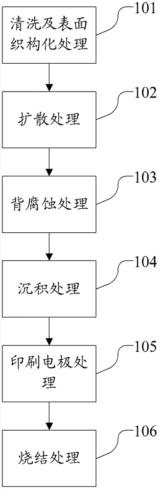
[0022] An embodiment of the present invention provides an edge etching process applied to polycrystalline silicon solar cells, which is used to replace the back etching process in the current manufacturing process of polycrystalline silicon solar cells. Using this edge etching process, the etching width can be about 50 microns, improve the effective use area of ​​the PN junction on the surface of the silicon wafer, and avoid the risk of using strong corrosive acid.

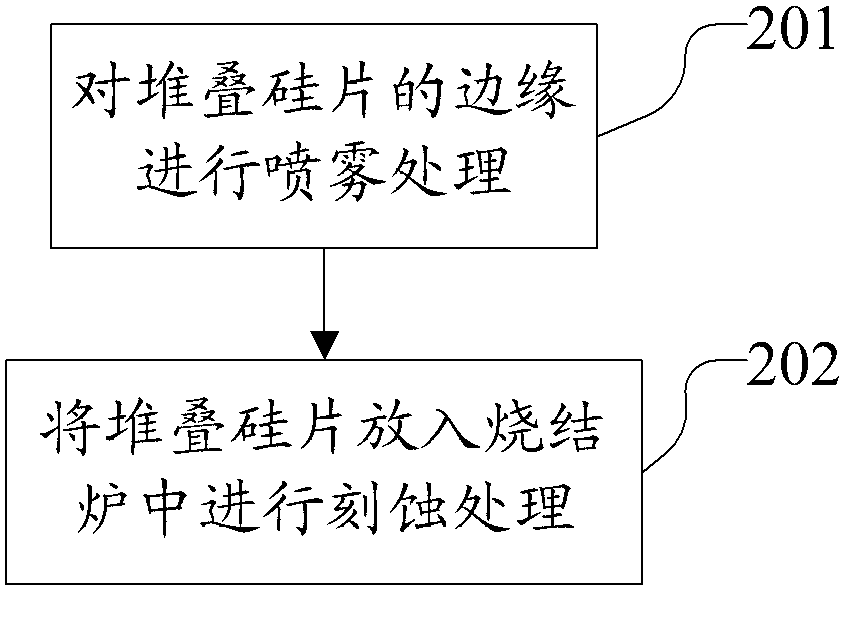
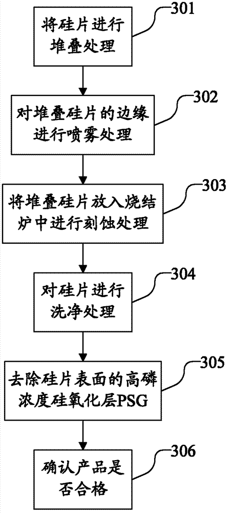
[0023] In the first embodiment of the present invention, please refer to figure 2 ,mainly include:

[0024] 201. Perform spray treatment on the edges of the stacked silicon wafers.

[0025] This step is carried out in a spray chamber, usually hundreds of silicon wafers are sprayed at the same time, these hundreds of silicon wafers will be processed into stacked silicon wafers, and then the edges of the stacked silicon wafers are sprayed. When spraying, the nozzles are used to spray the surrounding edges of the ...


PUM


Abstract

The invention discloses an edge etching process applied to a polycrystalline silicon solar cell. The edge etching process applied to the polycrystalline silicon solar cell is used for replacing back etching processing steps currently used in a manufacturing process of the polycrystalline silicon solar cell. The implementation method includes that edges of piled silicon slices are handled in an atomized mode, etching slurry for handling of atomizing is compound slurry which can corrode silicon and silica. The atomized piled silicon slices are put into a sintering furnace to be handled in an etched mode so that the etching slurry and the piled silicon slices react fully. By utilization of the edge etching process, the etching width can be about 50 microns, the effective utilization area of a PN junction is enlarged, and the risk of using strong-corrosiveness acid is avoided.

Description

technical field [0001] The invention relates to the technical field of solar energy, in particular to an edge etching process applied to polycrystalline silicon solar cells. Background technique [0002] In the field of solar energy technology, the basic process of the manufacturing process of polycrystalline silicon solar cells has been standardized. For the main steps, please refer to figure 1 ,include: [0003] 101. Cleaning and surface texturing treatment: After the silicon wafer is cleaned, the surface of the silicon wafer forms an uneven structure through a chemical reaction, which reduces surface reflection and increases the irradiation area. [0004] 102. Diffusion treatment: phosphorus oxychloride POCL on the surface of P-type silicon wafer 3 Diffusion transforms the surface of the P-type silicon wafer into N-type, thereby forming a PN junction, and the silicon wafer can convert solar energy into electrical energy by using the photovoltaic effect. [0005] 103. B...

Claims


Application Information

Patent Timeline
Patent Type & Authority Applications(China)
IPC IPC(8): H01L31/18
CPCY02P70/521Y02P70/50
Inventor 王志超
Owner JETION SOLAR HLDG
Why Eureka
Try Eureka