
Integrated circuit design and testing

a technology of integrated circuits and integrated circuits, applied in the direction of cad circuit design, program control, instruments, etc., can solve the problems of increasing the likelihood and potentially destructive effects of electrostatic discharge in ics, and achieve the effect of improving ttm

Inactive Publication Date: 2007-06-26
INTEL CORP
View PDF7 Cites 6 Cited by
  • Summary
  • Abstract
  • Description
  • Claims
  • Application Information

AI Technical Summary

Benefits of technology

[0011]Embodiments of the present invention offer a novel approach both to ensure RFT design and improve TTM in the area of ESD design. The invention provides a means by which non-ESD specialists can test their designs against pre-defined ESD strategies and by virtue of the nature of ESD protection for IC's, search for potential latent design weaknesses.

Problems solved by technology

The demand for fast Time To Market (TTM) and Right First Time (RFT) products in the field of semiconductor integrated circuits (ICs) is great in view of the high costs involved in state-of-the-art IC process technologies.
A significant barrier to achieving fast TTM and RFT products is the potentially destructive effects of electrostatic discharge in ICs, particularly as technologies become more complex and device geometries decrease.
However, a combination of ever more complex designs and advanced, high speed technologies with decreasing transistor breakdown voltages, is increasing the likelihood of alternative electrostatic discharge routes within the active circuit, switching on prior to a desired protection route.

Method used


Image

  • Integrated circuit design and testing
  • Integrated circuit design and testing
  • Integrated circuit design and testing

Examples


Embodiment Construction

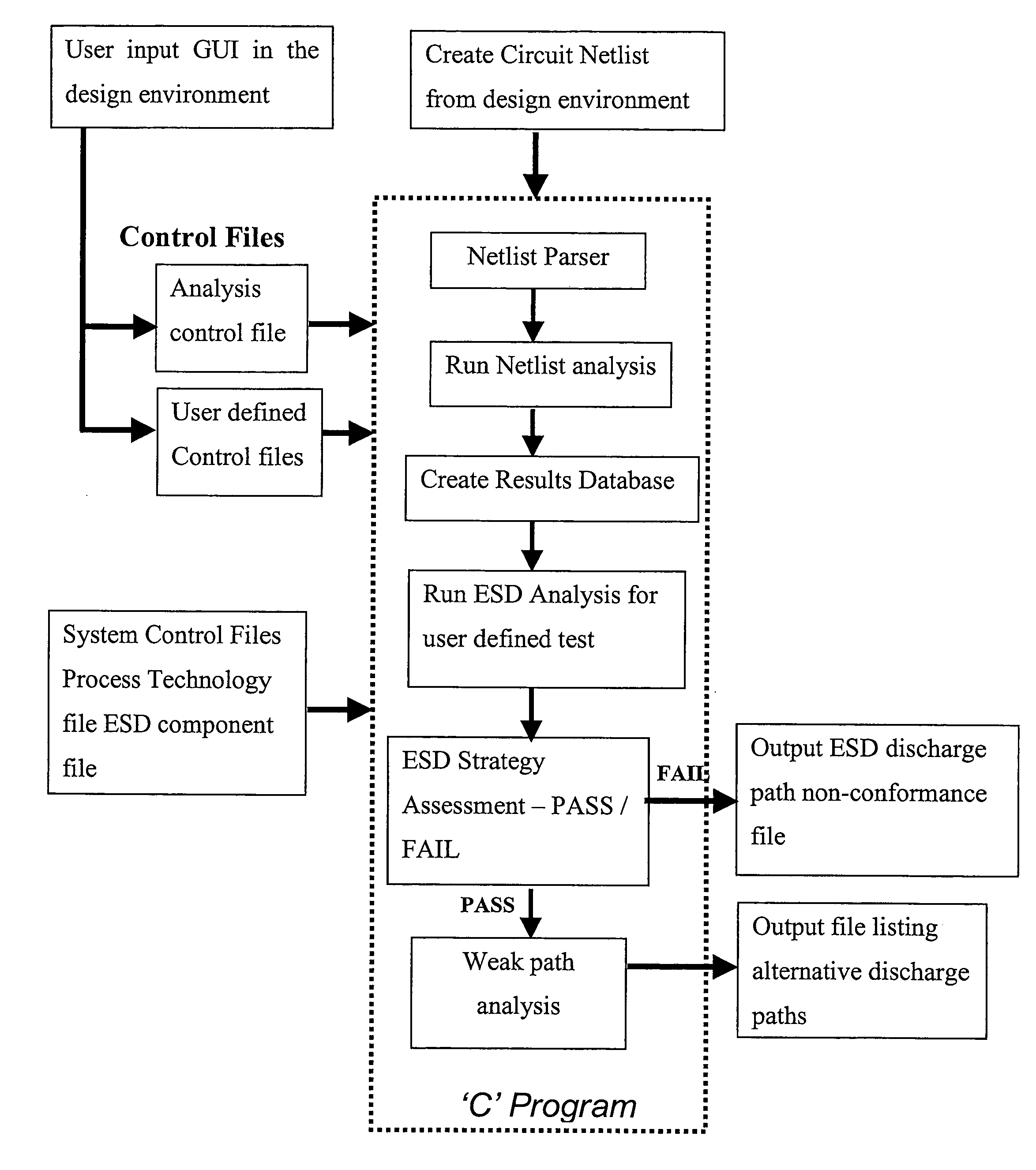
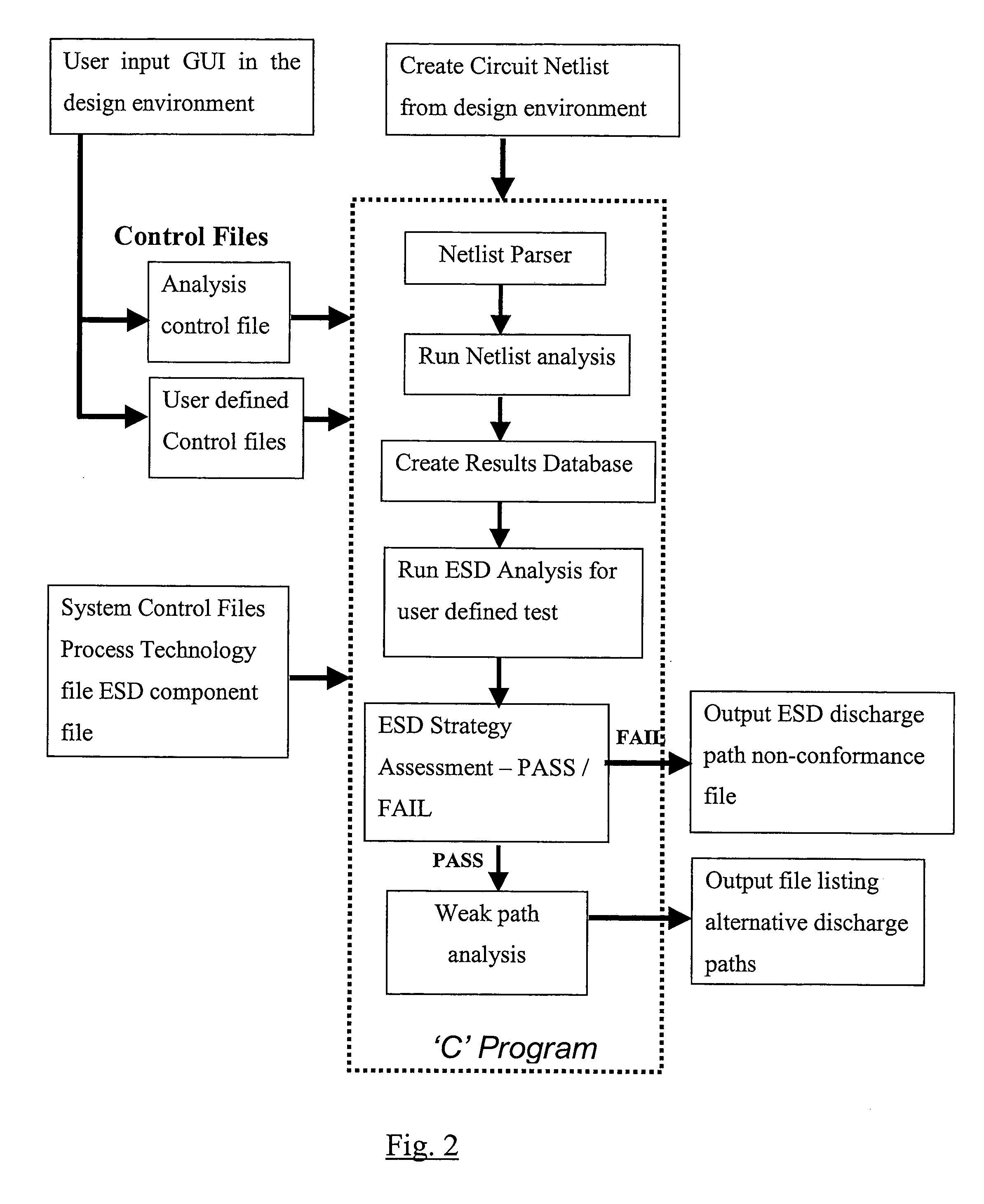
[0019]It has been explained above that a serious limitation of existing techniques for identifying weaknesses in electrostatic discharge (ESD) protection is the need for a manual analysis of large complex circuit networks. Ideally, this process should be computerised to both ensure accuracy and to extend the analysis to provide a RFT approach. The process described here is designed for implementation by computer, and relies on an in depth knowledge of the ESD process, particularly in terms of understanding the multitude of breakdown mechanisms possible, and of the ESD testing methodology required. This analysis, utilised with proven success, is based only on DC model parameters and does not require complex transient ESD models of components.

[0020]Combining DC model parameters for a given process technology with novel techniques for traversing and simplifying circuit netlists (i.e. lists of components and their connections), it has been possible to develop this technique into an auto...


PUM


Abstract

A method of testing an integrated circuit design to determine whether or not the design satisfies an electrostatic discharge protection specification, said circuit design incorporating electrostatic discharge protection routes between top-level nodes of the design. The method comprises defining an electrostatic discharge protection score for each of said electrostatic discharge protection routes, for each top-level node pair, calculating an electrostatic discharge score for every route through the active circuit between the top-level nodes, and identifying active circuit routes between top-level node pairs for which the electrostatic discharge score is less than the electrostatic discharge protection score for the corresponding electrostatic discharge protection route, or lies within a predefined amount of that score.

Description

FIELD OF THE INVENTION [0001]The present invention relates to the design and testing of integrated circuits. More particularly, the invention relates to aspects of the design and testing of integrated circuits relating to electrostatic discharge protection.BACKGROUND OF THE INVENTION [0002]The demand for fast Time To Market (TTM) and Right First Time (RFT) products in the field of semiconductor integrated circuits (ICs) is great in view of the high costs involved in state-of-the-art IC process technologies. A significant barrier to achieving fast TTM and RFT products is the potentially destructive effects of electrostatic discharge in ICs, particularly as technologies become more complex and device geometries decrease. Hence, in any IC design process a circuit strategy to prevent failure due to electrostatic discharge should be implemented.[0003]There are a number of standards organisations, for example JEDEC (Joint Electron Device Engineering Council), Solid State Technology Associ...

Claims


Application Information

Patent Timeline
Patent Type & Authority Patents(United States)
IPC IPC(8): G06F17/50G06F9/45
CPCG06F17/5045G06F30/30
Inventor STRICKLAND, KEITH R.CHADFIELD, STEPHEN R.O'CONNELL, JOHN B.
Owner INTEL CORP
Learn More