

Integrated circuit design and testing
- Summary
- Abstract
- Description
- Claims
- Application Information
AI Technical Summary
Benefits of technology
Problems solved by technology
Method used
Image

Examples
Embodiment Construction
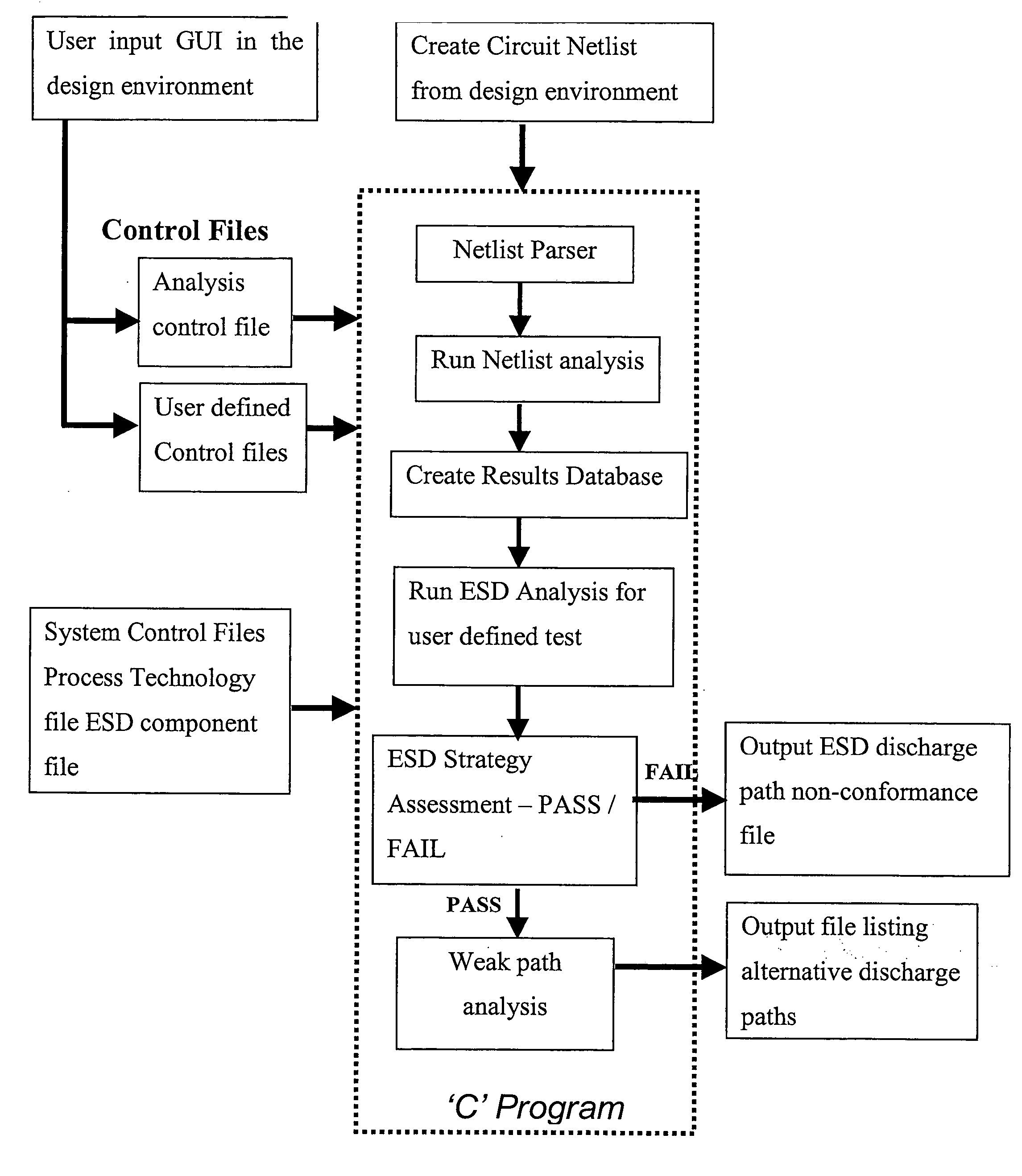
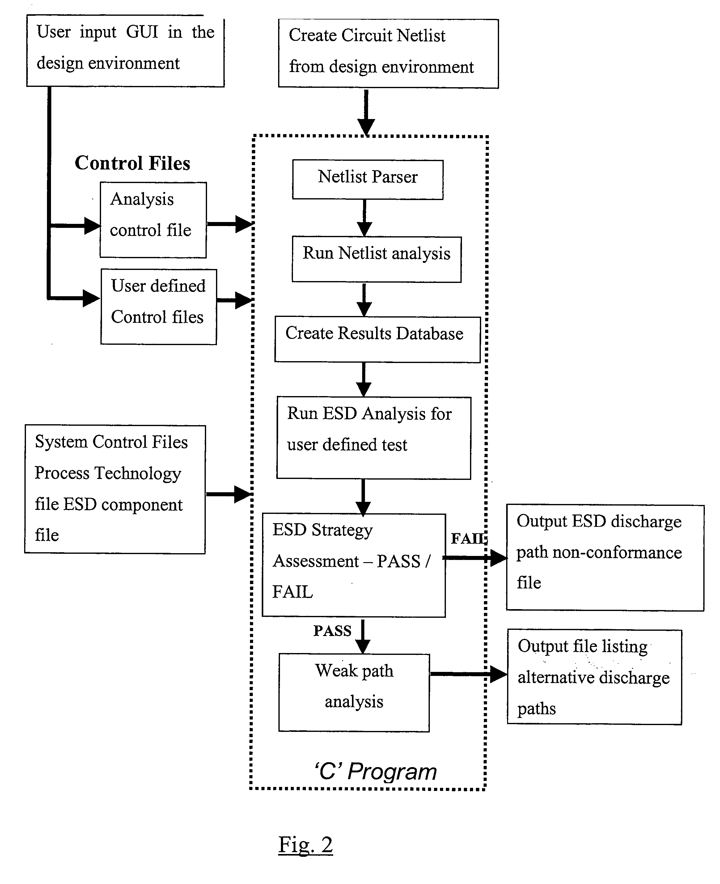
[0019] It has been explained above that a serious limitation of existing techniques for identifying weaknesses in electrostatic discharge (ESD) protection is the need for a manual analysis of large complex circuit networks. Ideally, this process should be computerised to both ensure accuracy and to extend the analysis to provide a RFT approach. The process described here is designed for implementation by computer, and relies on an in depth knowledge of the ESD process, particularly in terms of understanding the multitude of breakdown mechanisms possible, and of the ESD testing methodology required. This analysis, utilised with proven success, is based only on DC model parameters and does not require complex transient ESD models of components.
[0020] Combining DC model parameters for a given process technology with novel techniques for traversing and simplifying circuit netlists (i.e. lists of components and their connections), it has been possible to develop this technique into an a...
PUM
 Abstract
Description
Claims
Application Information