Method for forming a planar mirror using a sacrificial oxide
a technology of sacrificial oxide and planar mirror, which is applied in the direction of photomechanical equipment, instruments, originals for photomechanical treatment, etc., can solve the problems of providing an unacceptably low planar surface percentage of the mirror plate for reliable reflection, and the proportion of the deformed mirror plate that is distorted to provide an attachment point of similar siz
- Summary
- Abstract
- Description
- Claims
- Application Information
AI Technical Summary
Benefits of technology
Problems solved by technology
Method used
Image
Examples
example micro -
Example Micro-Mirror Device
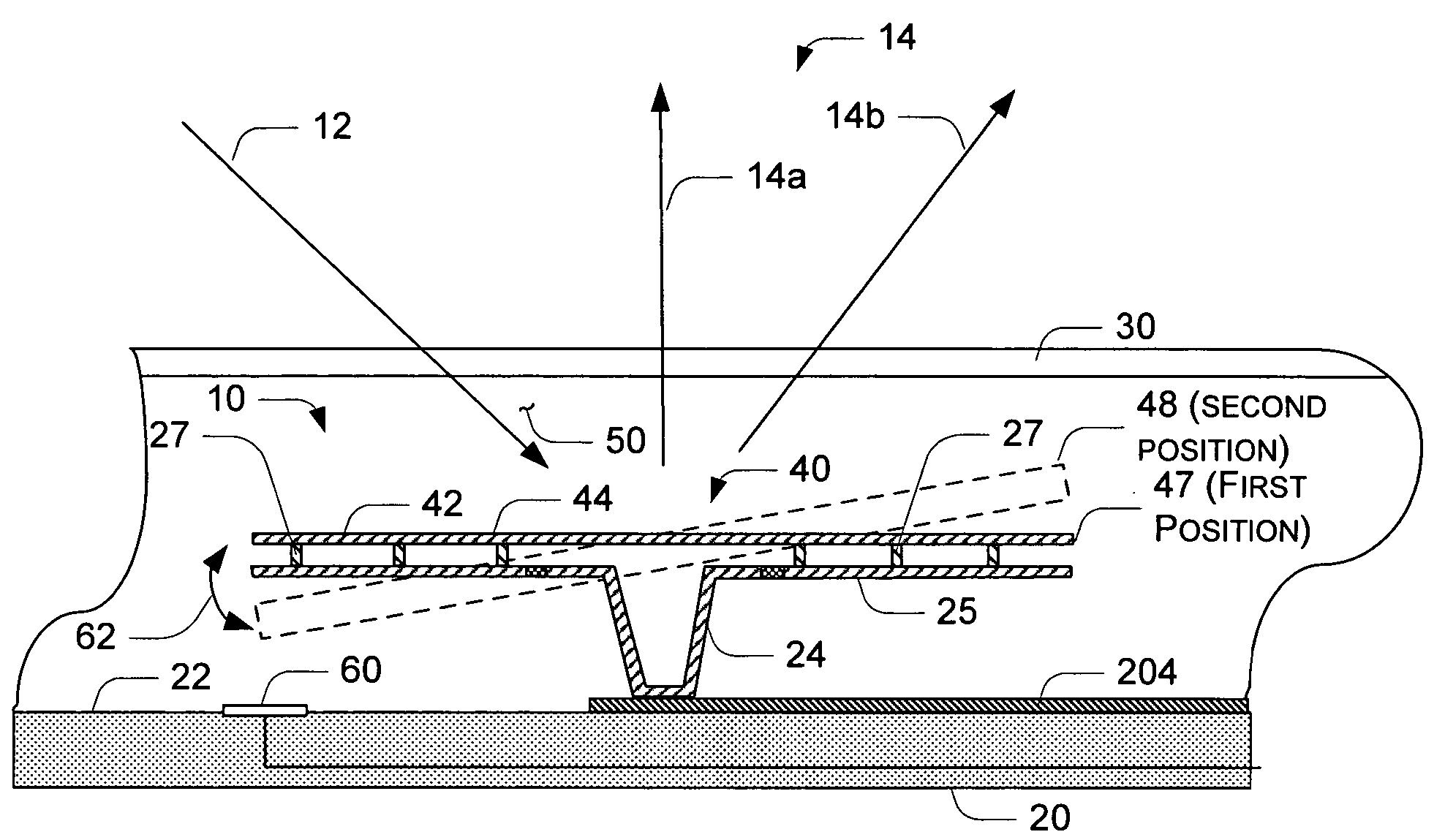
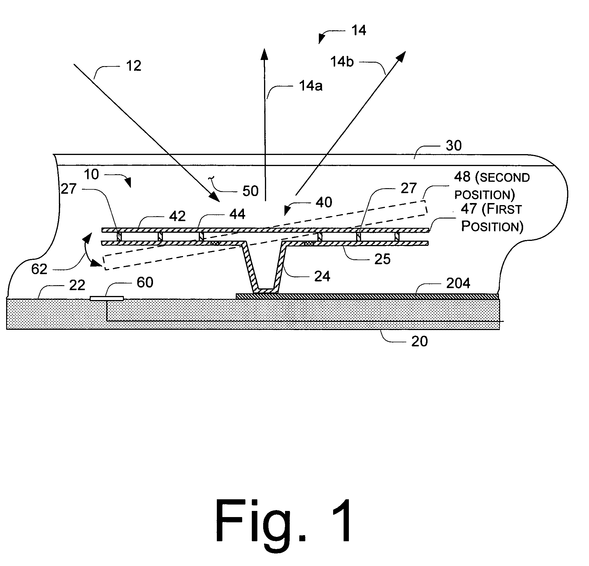
[0010]With reference to FIG. 1, the micro-mirror device 10 is formed on a substrate 20 and lies underneath a coverplate 30. One embodiment of the micro-mirror device 10 comprises at least some of an actuator element 40, a support 24, a hinged member 25, the mirror plate 42, a plurality of mirror support elements 27, and an electrode 60. The actuator element 40 acts as a micro-actuator that utilizes electrical to mechanical conversion to generate a force and cause movement or actuation of the mirror plate 42 relying on the flexibility of the hinged member 25. The hinged member 25 is formed with one or more hinges (shown in checkered cross-section in FIG. 1) that allow the hinged member 25 to be displaced during actuation. In the illustrated and described embodiment, the mirror plate 42 is angularly displaceable from a first position 47 that is substantially parallel to a surface of the substrate 20 to a second position as a result of displacement of the hin...
example micro
-Mirror Device Fabrication
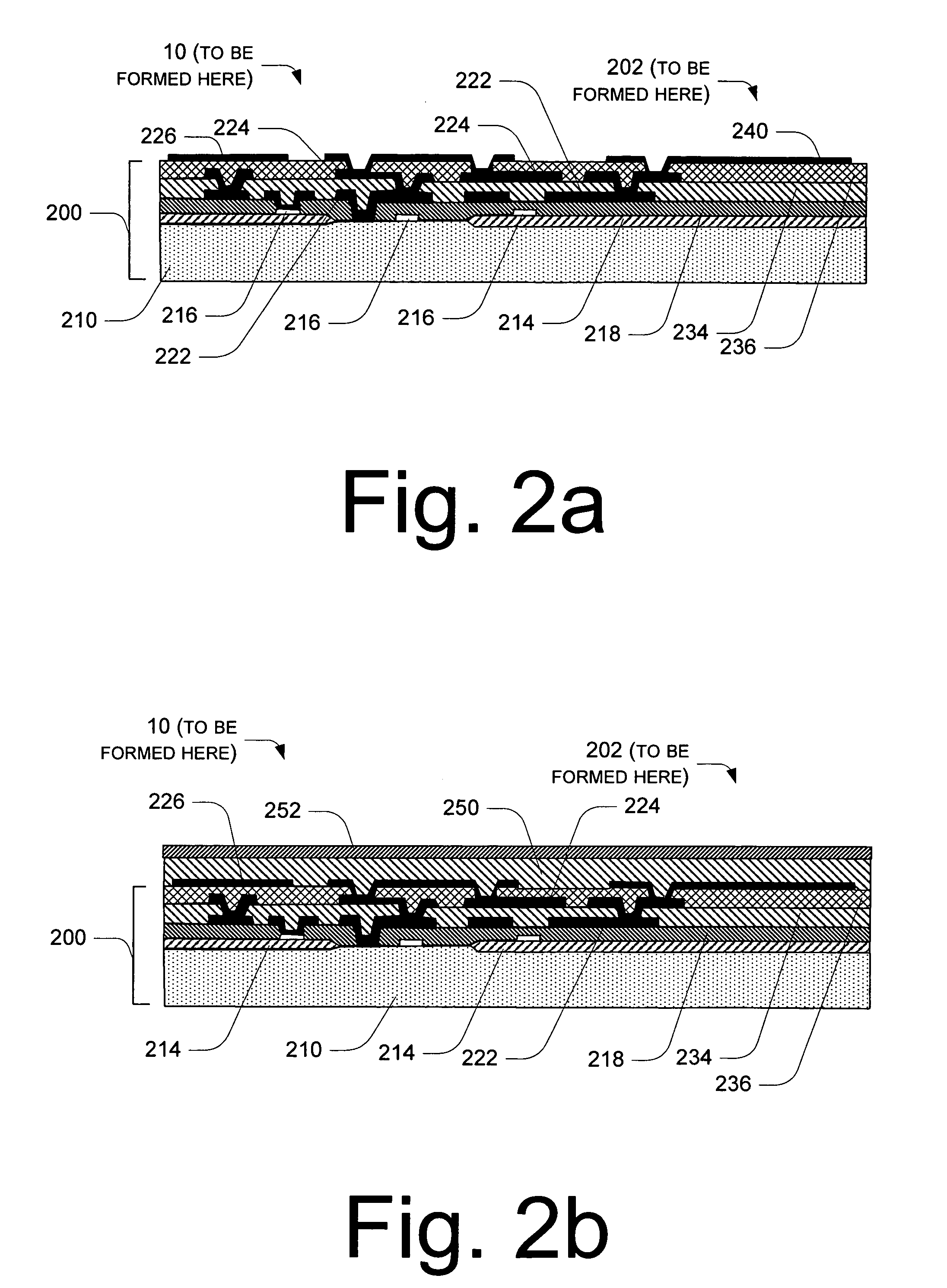
[0023]FIGS. 2a-2h illustrate one embodiment of an example of a fabrication process that produces the micro-mirror device 10 as shown in FIG. 1 in combination with an electrical contact area 202 at which electricity that is applied to a sub-structure 200. Electrical signals that are applied to the electrical contact area 202 can be selectively applied to the desired locations of the micro-mirror device 10 based on well understood integrated circuit layouts and operations. The fabrication process of FIGS. 2a-2h can involve simultaneous processing steps at the micro-mirror device 10 and the electrical contact area 202. The fabrication process starts with fabricating a sub-structure 200 as illustrated in FIG. 2a. In one embodiment, the sub-structure 200 includes a complementary metal oxide semi-conductor (CMOS) structure with a desired semiconductor and metal configuration. In an exemplary embodiment, the CMOS structure includes a multi-level metal CMOS circuit...
PUM
 Abstract
Description
Claims
Application Information


