Light emitting device and electronic appliance

a technology of light emitting devices and electronic appliances, which is applied in the field of oled panels, can solve the problems of reducing the luminance of the oled according, affecting the quality of the final product, and affecting the quality of the final product, and achieves the effect of constant luminan

Inactive Publication Date: 2008-02-26
SEMICON ENERGY LAB CO LTD
View PDF31 Cites 41 Cited by
  • Summary
  • Abstract
  • Description
  • Claims
  • Application Information

AI Technical Summary

Benefits of technology

[0014]Accordingly, in view of the above-mentioned circumstances, an object of the present invention is to provide a light emitting device capable of obtaining a constant luminance regardless of the organic light emitting layer deterioration or the temperature change, and further capable of providing a desired color display.
[0015]The present inventor has paid attention to the fact that the OLED luminance decline by the deterioration is smaller in the latter case in comparison between the light emission with the OLED driving voltage maintained constantly (the former case) and the light emission with the current flowing in the OLED maintained constantly (the latter case). In this specification, the current flowing in the OLED is referred to as the OLED driving current (Ie1). Then, it is considered that the change of the OLED luminance by the OLED deterioration can be prevented by controlling the OLED luminance not by the voltage but by the current.
[0020]In the present invention, according to the above-mentioned configuration, decline of the luminance of the OLED can be restrained even in the case the organic light emitting layer is deteriorated, and as a result, a sharp image can be displayed. Moreover, in the case of a color display light emitting device using the OLED corresponding to each color, even in the case the organic light emitting layers of the OLED are deteriorated by different rates per each corresponding color, a desired color can be displayed by preventing deterioration of the balance of the luminance among the colors.
[0021]Furthermore, even in the case the temperature of the organic light emitting layer is influenced by the external atmosphere temperature, the heat generated by the OLED panel itself, or the like, the OLED driving current can be controlled at a desired value. Therefore, since the OLED driving current and the luminance of the OLED are proportional, change of the luminance of the OLED can be restrained, and further, increase of the current consumption according to the temperature rise can be prevented. Moreover, in the case of a color display light emitting device, since change of the luminance of the OLED of each color can be restrained regardless of the temperature change, deterioration of the balance of the luminance among the colors can be prevented so that a desired color can be displayed.
[0022]Furthermore, in general, since the degree of the change of the OLED driving current in the temperature change differs depending on the kind of the organic light emitting material, the luminance of the OLED of each color can be changed independently in the color display. However, according to the light emitting device of the present invention, since a desired luminance can be obtained regardless of the temperature change, deterioration of the balance of the luminance among the colors can be prevented so that a desired color can be displayed.

Problems solved by technology

It has been problematic at the time of putting the light emitting device into practice that the luminance of the OLED is lowered according to deterioration of the organic light emitting material.
Accordingly, since the luminance of the OLED is changed depending on the temperature of the organic light emitting layer, it is difficult to display a desired gradient so that the current consumption of the light emitting device is enlarged according to the temperature rise.

Method used


Image

  • Light emitting device and electronic appliance
  • Light emitting device and electronic appliance
  • Light emitting device and electronic appliance

Examples


embodiment 1

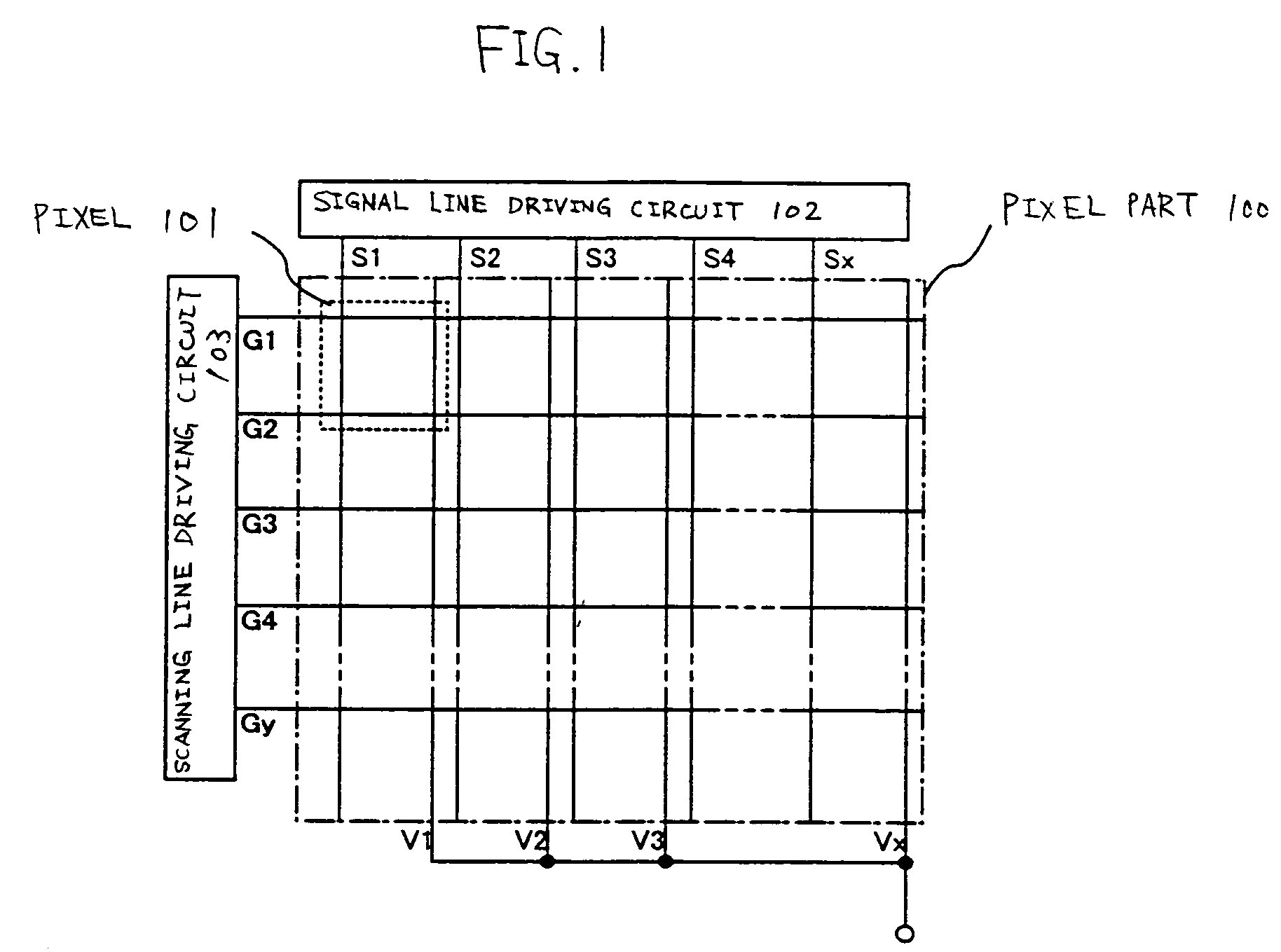
[0056]FIG. 1 is a block diagram showing the configuration of an OLED panel of the present invention. The numeral 100 is a pixel part, with a plurality of pixels 101 formed in a matrix-like form. Moreover, the numeral 102 is a signal line driving circuit, and the numeral 103 is a scanning line driving circuit.

[0057]Although the signal line driving circuit 102 and the scanning line driving circuit 103 are formed on the same substrate as the pixel part 100 in FIG. 1, the present invention is not limited to the configuration. It is possible that the signal line driving circuit and the scanning line driving circuit 103 are formed on a substrate different from that of the pixel part 100, and connected with the pixel part 100 via a connector such as an FPC. Moreover, although the signal line driving circuit 102 and the scanning line driving circuit 103 are provided one by one in FIG. 1, the present invention is not limited to the configuration. The number of the signal line driving circuit...

embodiment 2

[0097]In this embodiment, a configuration of the pixel 101 shown in FIG. 1 different from that of FIG. 2 will be explained.

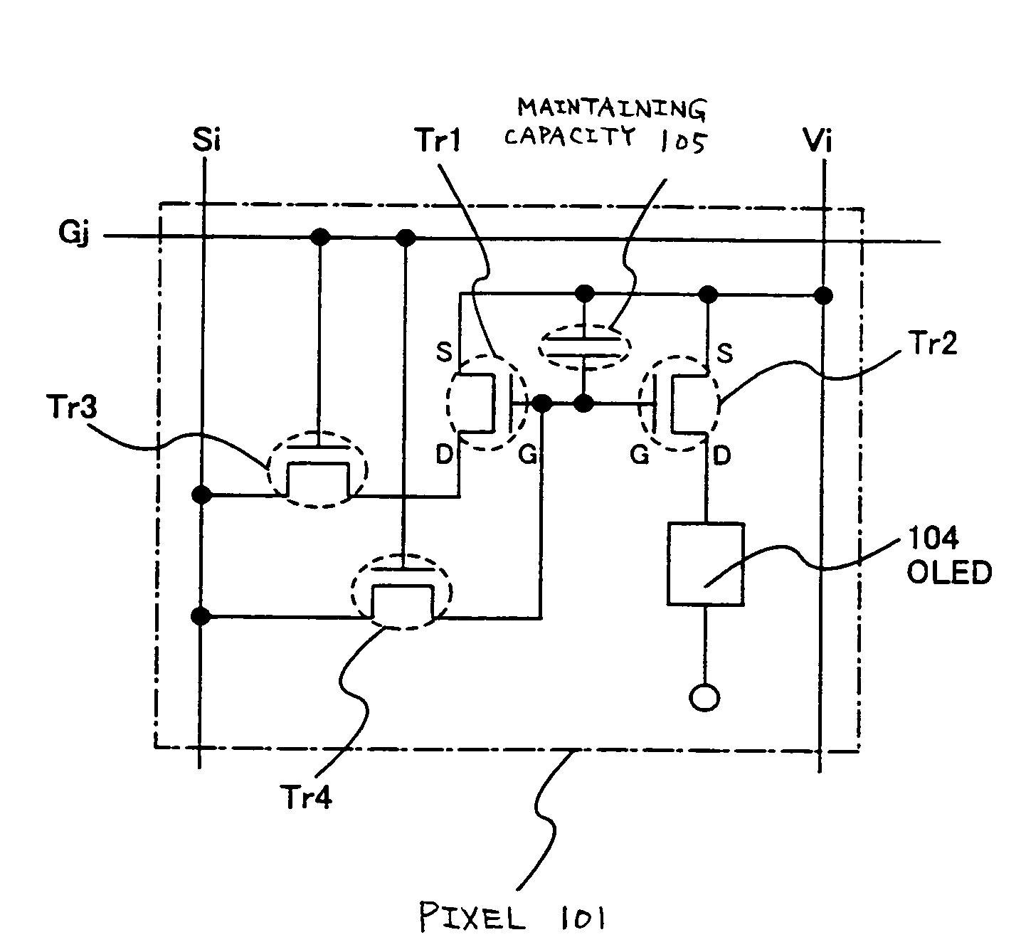
[0098]FIG. 7 shows the configuration of the pixel of this embodiment. The pixel 101 shown in FIG. 7 has a signal line Si (one from Sl to Sx), a scanning line Gj (one from G1 to Gy), and a power source line Vi (one from V1 to Vx).

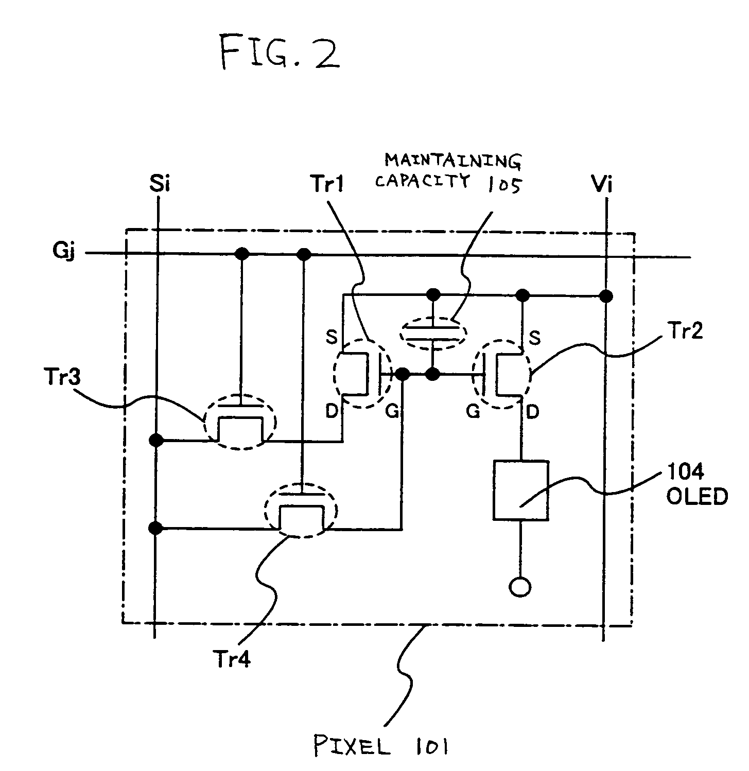
[0099]Moreover, the pixel 101 comprises at least a transistor Tr1 (first current driving transistor), a transistor Tr2 (second current driving transistor), a transistor Tr3 (first switching transistor), a transistor Tr4 (second switching transistor), an OLED 104 and a maintaining capacity 105.

[0100]The gate electrodes of the transistor Tr3 and the transistor Tr4 are both connected with the scanning line Gj.

[0101]One of the source area and the drain area of the transistor Tr3 is connected with the signal line Si, and the other one is connected with the drain area of the transistor Tr1. Moreover, one of the source area and the drain area o...

embodiment 3

[0108]In this embodiment, a configuration of the pixel 101 shown in FIG. 1 different from that of FIG. 2 and FIG. 7 will be explained.

[0109]FIG. 8 shows the configuration of the pixel of this embodiment. The pixel 101 shown in FIG. 8 has a signal line Si (one from S1 to Sx), a scanning line Gj (one from G1 to Gy), and a power source line Vi (one from V1 to Vx).

[0110]Moreover, the pixel 101 comprises at least a transistor Tr1 (first current driving transistor), a transistor Tr2 (second current driving transistor), a transistor Tr3 (first switching transistor), a transistor Tr4 (second switching transistor), an OLED 104 and a maintaining capacity 105.

[0111]The gate electrodes of the transistor Tr3 and the transistor Tr4 are both connected with the scanning line Gj.

[0112]One of the source area and the drain area of the transistor Tr3 is connected with the signal line Si, and the other one is connected with the gate electrode of the transistor Tr1. Moreover, one of the source area and t...


PUM

PropertyMeasurementUnit
thicknessaaaaaaaaaa
thicknessaaaaaaaaaa
thicknessaaaaaaaaaa

Abstract

The present invention is to provide a light emitting device capable of obtaining a certain luminance without influence by the temperature change, and a driving method thereof. A current mirror circuit formed by using a transistor is provided for each pixel. The first transistor and the second transistor of the current mirror circuit are connected such that the drain currents thereof are maintained at proportional values regardless of the load resistance value. Thereby, a light emitting device capable of controlling the OLED driving current and the luminance of the OLED by controlling the drain current of the first transistor at a value corresponding to a video signal in a driving circuit, and supplying the drain current of the second transistor to the OLED, is provided.

Description

CROSS-REFERENCE TO RELATED APPLICATIONS[0001]This application is a continuation application (and claims the benefit of priority under 35 USC 120) of U.S. application Ser. No. 10 / 077,830, filed Feb. 20, 2002, now allowed, U.S. Pat. No. 6,753,654 which claims the benefit of a foreign priority application filed in Japan as Serial No. 2001-045644 on Feb. 21, 2001. This application claims priority to both of these applications, and both of these applications are incorporated by reference.BACKGROUND OF THE INVENTION[0002]1. Field of the Invention[0003]The present invention relates to an OLED panel having an organic OLED (OLED: organic light emitting device) formed on a substrate, sealed between the substrate and a cover material. Moreover, it relates to an OLED module having an IC, or the like including a controller packaged on the OLED panel. In this specification, both the OLED panel and the OLED module are referred to as the light emitting device. Furthermore, the present invention rel...

Claims


Application Information

Patent Timeline
Patent Type & Authority Patents(United States)
IPC IPC(8): G09G3/10C09K11/06G09G3/20H01L27/32H05B33/14
CPCC09K11/06H01L27/3272G09G3/2022G09G3/3241G09G3/3266G09G3/3283H05B33/14H01L27/3246H01L27/3258C09K2211/185G09G2300/0417G09G2300/0426G09G2300/0809G09G2300/0842G09G2300/0861G09G2310/027G09G2320/0247G09G2320/0266G09G2320/041H01L27/3244C09K2211/1088G09G2310/0272Y02E10/549Y02P70/50H10K59/12H10K50/846H10K59/122H10K59/123H10K59/124H10K59/126H10K59/1213H10K59/1315H10K77/10H10K2102/00G09G3/3208H01L27/1222H01L27/1285
Inventor KOYAMA, JUN
Owner SEMICON ENERGY LAB CO LTD
Why Eureka
Try Eureka