Current biased dual DBR grating semiconductor laser

a semiconductor laser and current biased technology, applied in the direction of laser details, laser optical resonator construction, optical resonator shape and construction, etc., can solve the problems of large and complex chip design, difficult to select and tune a wavelength, and unaffected other wavelength(s) , to achieve the effect of reducing the added cavity loss of the back grating mode, reducing the coupling coefficient and reducing the current induced thermal interaction

Inactive Publication Date: 2008-03-04
THE BOARD OF TRUSTEES OF THE UNIV OF ILLINOIS
View PDF22 Cites 3 Cited by
  • Summary
  • Abstract
  • Description
  • Claims
  • Application Information

AI Technical Summary

Benefits of technology

[0006]In the present laser, dual-wavelength operation is easily achieved by biasing the gain section. Multiple gratings spaced apart from each other are separated from an output aperture by a gain section. A relatively low coupling coefficient, K, in the front grating reduces the added cavity loss for the back grating mode. Therefore, the back grating mode reaches threshold easily. The space section lowers the current induced thermal interaction between the two uniform grating sections, significantly reducing the inadvertent wavelength drift. As a result, a tunable mode pair separations (Δλ) as small as 0.3 nm and as large as 6.9 nm can be achieved.

Problems solved by technology

This can lead to large and complex chip design, however.
Such integrated design of the multi wavelength feedback makes it difficult to select and tune a wavelength while leaving other wavelength(s) unaffected.

Method used


Image

  • Current biased dual DBR grating semiconductor laser
  • Current biased dual DBR grating semiconductor laser
  • Current biased dual DBR grating semiconductor laser

Examples


Embodiment Construction

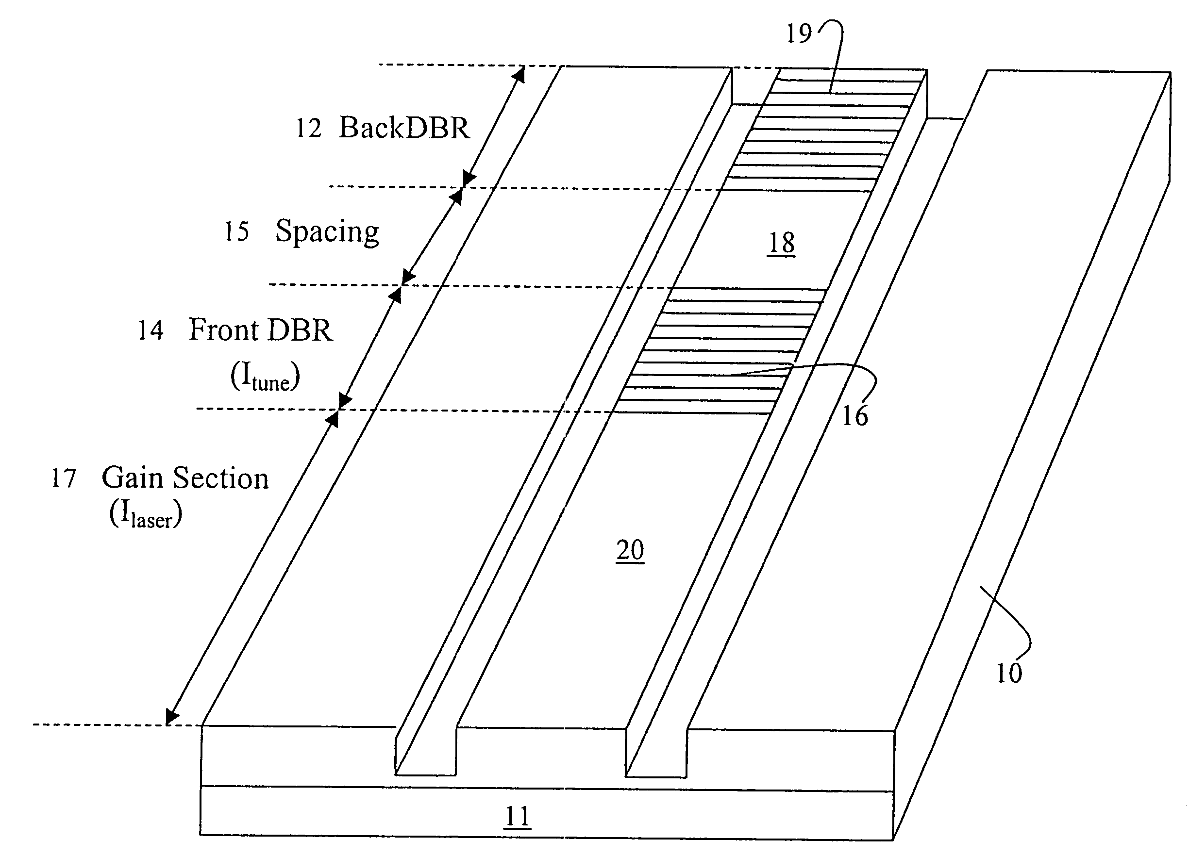
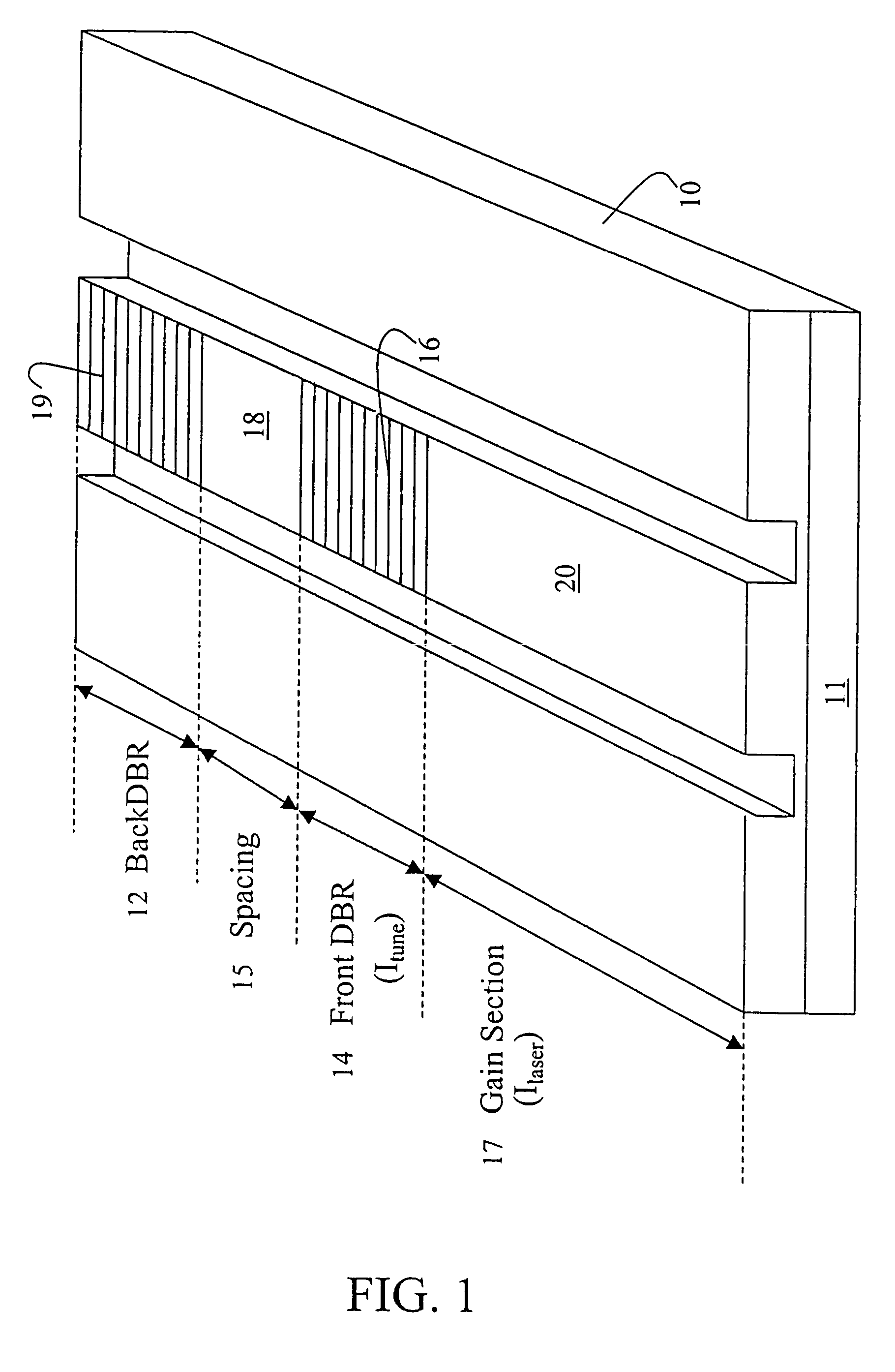
[0011]Referring now to FIG. 1, a preferred ridge waveguide-distributed Bragg reflector (RW-DBR) laser heterostructure 10 of the invention is shown. The laser heterostructure emits from an output aperture 11. A rear surface distributed Bragg grating 12 is formed on a surface of said laser heterostructure. The laser also includes a front surface distributed Bragg grating 14 on a surface of said laser heterostructure. The front surface distributed Bragg grating 14 is closer to the output aperture 11 than the rear surface distributed Bragg grating 12. There is a space 15 between the rear surface distributed Bragg grating 12 and the front surface distributed Bragg grating 14. A tuning electrode 16 is formed on the front surface distributed Bragg grating 14, and the region between the front distributed Bragg grating and the output aperture 11 forms a gain section 17. A current drive electrode 18 is formed on the space 15, and a tuning electrode 19 on the rear surface distributed Bragg gra...


PUM


Abstract

Dual-wavelength operation is easily achieved by biasing the gain section. Multiple gratings spaced apart from each other are separated from an output aperture by a gain section. A relatively low coupling coefficient, κ, in the front grating reduces the added cavity loss for the back grating mode. Therefore, the back grating mode reaches threshold easily. The space section lowers the current induced thermal interaction between the two uniform grating sections, significantly reducing the inadvertent wavelength drift. As a result, a tunable mode pair separations (Δλ) as small as 0.3 nm and as large as 6.9 nm can be achieved.

Description

REFERENCE TO RELATED APPLICATION AND PRIORITY CLAIM[0001]This application is a continuation application of and related to U.S. application Ser. No. 09 / 660,611, filed on Sep. 13, 2000, now U.S. Pat. No. 6,728,290, and claims priority from that application under 35 U.S.C. §120.STATEMENT OF GOVERNMENT INTEREST[0002]This invention was made with government assistance under National Science Foundation grant ECS 99-00258 and the Air Force Office of Scientific Research contract F49620-96-1-0163 COL. The Government has certain rights in this invention.FIELD OF THE INVENTION[0003]The field of the invention is semi conductor lasers.BACKGROUND OF THE INVENTION[0004]Multiwavelength optical sources are important components in applications such as wavelength division multiplexing, optical remote sensing, and optical data processing. Multiple wavelengths are commonly achieved from a single output by integrating the output from multiple, discrete lasers. This can lead to large and complex chip desig...

Claims


Application Information

Patent Timeline
Patent Type & Authority Patents(United States)
IPC IPC(8): H01S5/00H01S3/08H01S3/10H01S5/0625H01S5/12H01S5/125H01S5/22
CPCH01S5/06256H01S5/22H01S5/1096H01S5/1206H01S5/1225H01S5/124H01S5/125
Inventor COLEMAN, JAMES J.ROH, S. DAVID
Owner THE BOARD OF TRUSTEES OF THE UNIV OF ILLINOIS
Why Eureka
Try Eureka