Spacer structure for image forming apparatus

a spacer structure and image forming technology, applied in the field of spacer structure for image forming apparatus, can solve the problem that the existence does not easily exercise an influence on the trajectory of an electron beam, and achieve the effect of suppressing cumulative charging, suppressing short charging time, and preventing deterioration of display characteristics

Inactive Publication Date: 2008-11-11
CANON KK
View PDF7 Cites 3 Cited by
  • Summary
  • Abstract
  • Description
  • Claims
  • Application Information

AI Technical Summary

Benefits of technology

[0008]It is an object of the invention to provide an image forming apparatus that can suppress cumulative charging in a spacer on which a rough surface is formed and which suppresses the short time charging and prevents deterioration in display characteristics due to a change in beam spot position due to such suppression.

Problems solved by technology

A technical problem which the spacer has to satisfy is that not only an element as an atmospheric pressure resistance structure is necessary but also, in order to keep quality of a display image, it is necessary that its existence does not easily exercise an influence on a trajectory of an electron beam.

Method used


Image

  • Spacer structure for image forming apparatus
  • Spacer structure for image forming apparatus
  • Spacer structure for image forming apparatus

Examples


example 1

[0074]The spacers which are used in the invention are manufactured as follows.

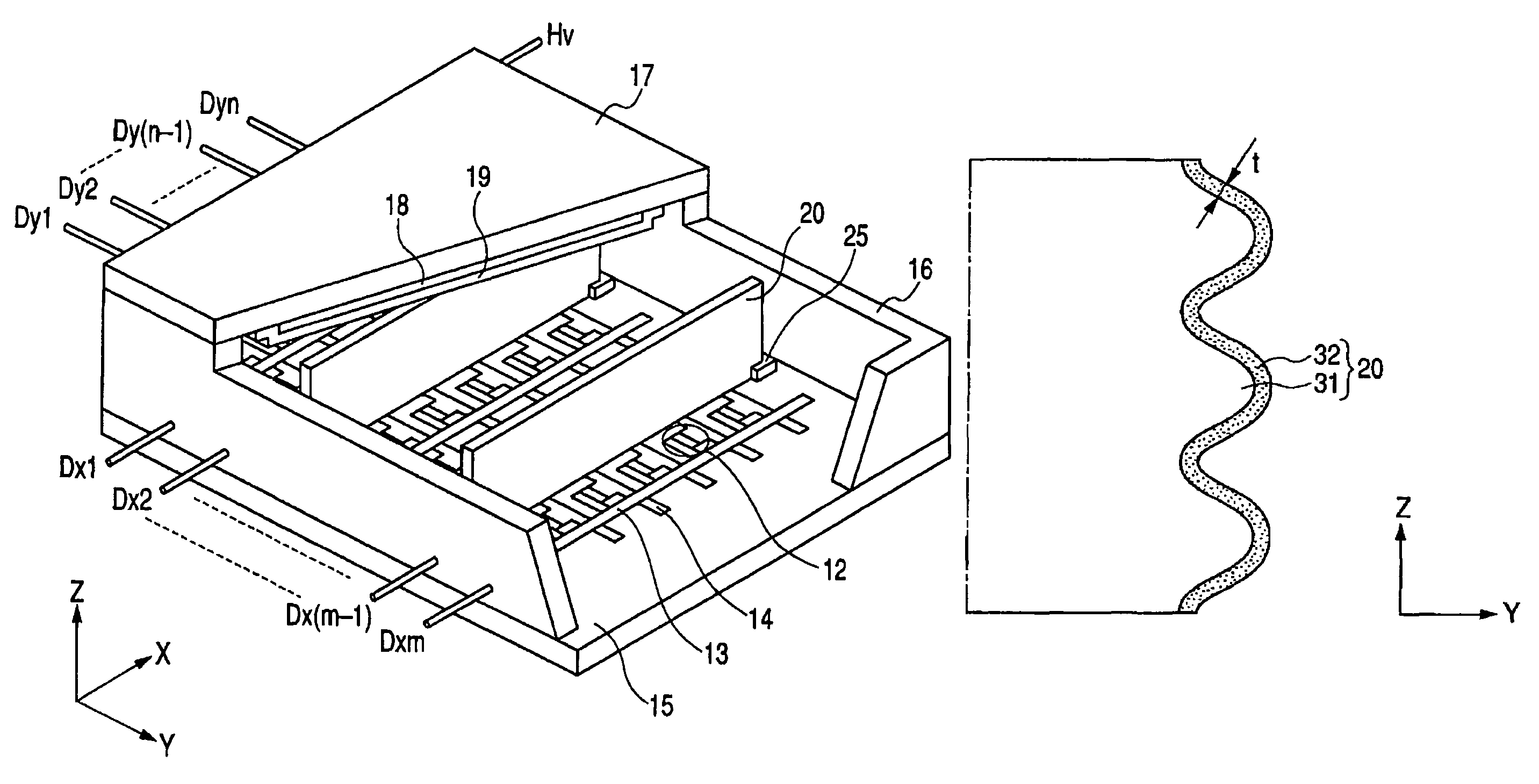
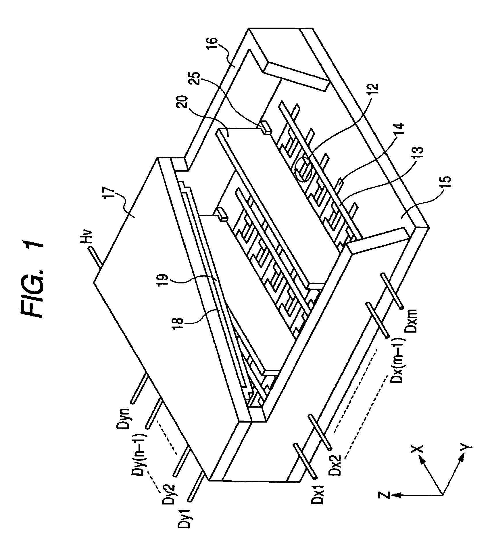
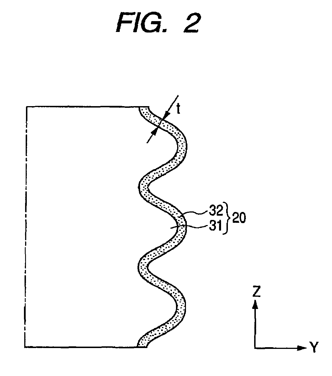
[0075]A substrate (PD200 made by Asahi Glass Co., Ltd.) is used as a base material and worked into a proper shape by a heat drawing method and a resultant plate is prepared as an insulating substrate of the spacer. The substrate has dimensions of (1.7 mm×0.18 mm×820 mm) and convex portions whose cross sectional shape is an almost trapezoid and whose average height is equal to 8 μm are formed at a pitch of 30 μm on the surface of (820 mm×1.7 mm) (hereinafter, referred to as a side surface). Surfaces of (0.18 mm×820 mm) (hereinafter, referred to as a contact surface) are formed in a flat shape so as to be come into contact with the cathode (upper wirings) and the anode (metal back). A corner between the side surface and the bottom surface is formed in a round shape so as to minimize the chipping and its radius of curvature is set to 5 μm. The concave and convex portions and the round shape of the corner port...

example 2

[0086]The spacer is formed and the image forming apparatus is constructed and driven in a manner similar to Example 1 except that the electrodes made of Pt are formed on the bottom surfaces (that is, two positions of the surfaces of 0.18 mm×820 mm) of the spacer. Thus, even if the apparatus is driven for a long time, a positional deviation of the electron beam near the spacer is not found. Further, it has been confirmed that, even in the depth region of the high resistance film on the spacer surface, the electric potential specification by the current field of the spacer is satisfied.

example 3

[0087]The spacer is formed and the image forming apparatus is constructed in a manner similar to Example 1 except that insulating layer (volume resistance at 25° C.: 3×10¹¹ Ωcm or more) of amorphous carbon is stacked and formed on the surface of the high resistance film so as to have a thickness of 10 nm. Thus, even if the apparatus is driven for a long time, a positional deviation of the electron beam near the spacer is not found. It has been confirmed that, even in the depth region of the high resistance film on the spacer surface, the electric potential specification by the current field of the spacer is satisfied.

[0088]A film density of the WGeN film of each of the high resistance films 2 of the spacers 1-1 and 1-4 in Example 1 is equal to 16 g / cm3 and a film density of the high resistance film 1 (PtAlN film) of the first layer is equal to 9.1 g / cm3. The film density is obtained by measuring the RBS: Rutherford Backscattering Spectrometory to determine the m value.

[0089]A method...


PUM


Abstract

In a spacer having concave / convex portions to prevent short-time charging in a flat type image forming apparatus in which an electron source substrate and an anode substrate are arranged so as to face each other through the spacer, the charging upon long-time driving due to the concave / convex portions is suppressed. In the spacer in which the surface of an insulating substrate having a rough surface is coated with a high resistance film, the high resistance film has double layers of a low resistance region locating on the substrate side and a high resistance region locating on the front surface side, and a thickness (t) of high resistance film on the slant surface of each of the concave / convex portions and a thickness (s) of high resistance region are set to (t≧dp+λ≧s) for the primary electron penetration length (dp) and the ionization electron diffusion length (λ).

Description

BACKGROUND OF THE INVENTION[0001]1. Field of the Invention[0002]The invention relates to an image forming apparatus such as a flat type image display apparatus or the like using electron-emitting devices and light emitting members and, more particularly, to the invention having a feature in a spacer which is interposed between an electron source substrate on which the electron-emitting devices are formed and a substrate having the light emitting-members in order to keep a distance between both of those substrates.[0003]2. Related Background Art[0004]Hitherto, as for an image display apparatus including a CRT, a further larger display screen is demanded and it is an important subject to realize a thin size and a light weight of the apparatus in association with the realization of the large display screen. As an image display apparatus which can realize the thin size and light weight, the applicant of the present invention has proposed the flat type image display apparatus using surfa...

Claims


Application Information

Patent Timeline
Patent Type & Authority Patents(United States)
IPC IPC(8): H01J1/62H01J63/04
CPCH01J29/864H01J31/127H01J2329/863H01J2329/8635H01J2329/864H01J2329/8645G03G15/04
Inventor ITO, NOBUHIRO
Owner CANON KK
Why Eureka
Try Eureka