Check patentability & draft patents in minutes with Patsnap Eureka AI!

Mask pattern and method for forming the same

a mask pattern and mask technology, applied in the field of mask pattern and method for forming the same, can solve the problems of assistant pattern, seriously affected device properties, and seriously affected electrical performance of the device, and achieve the effect of increasing the process window of the photolithography process

Active Publication Date: 2010-03-30
UNITED MICROELECTRONICS CORP
View PDF4 Cites 0 Cited by
  • Summary
  • Abstract
  • Description
  • Claims
  • Application Information

AI Technical Summary

Benefits of technology

This design effectively reduces corner rounding and end-cap shortening, enhances electrical stability, and simplifies database storage by preventing assistant patterns from being printed in the photoresist or material layer, thereby improving the photolithography process.

Problems solved by technology

Nevertheless, in the integrated circuit with high integration, the device properties are seriously affected.
Therefore, the electrical performance of the device is seriously affected.
However, additionally forming the assistant pattern would complicate the patterns on the mask.

Method used


Image

  • Mask pattern and method for forming the same
  • Mask pattern and method for forming the same
  • Mask pattern and method for forming the same

Examples


Embodiment Construction

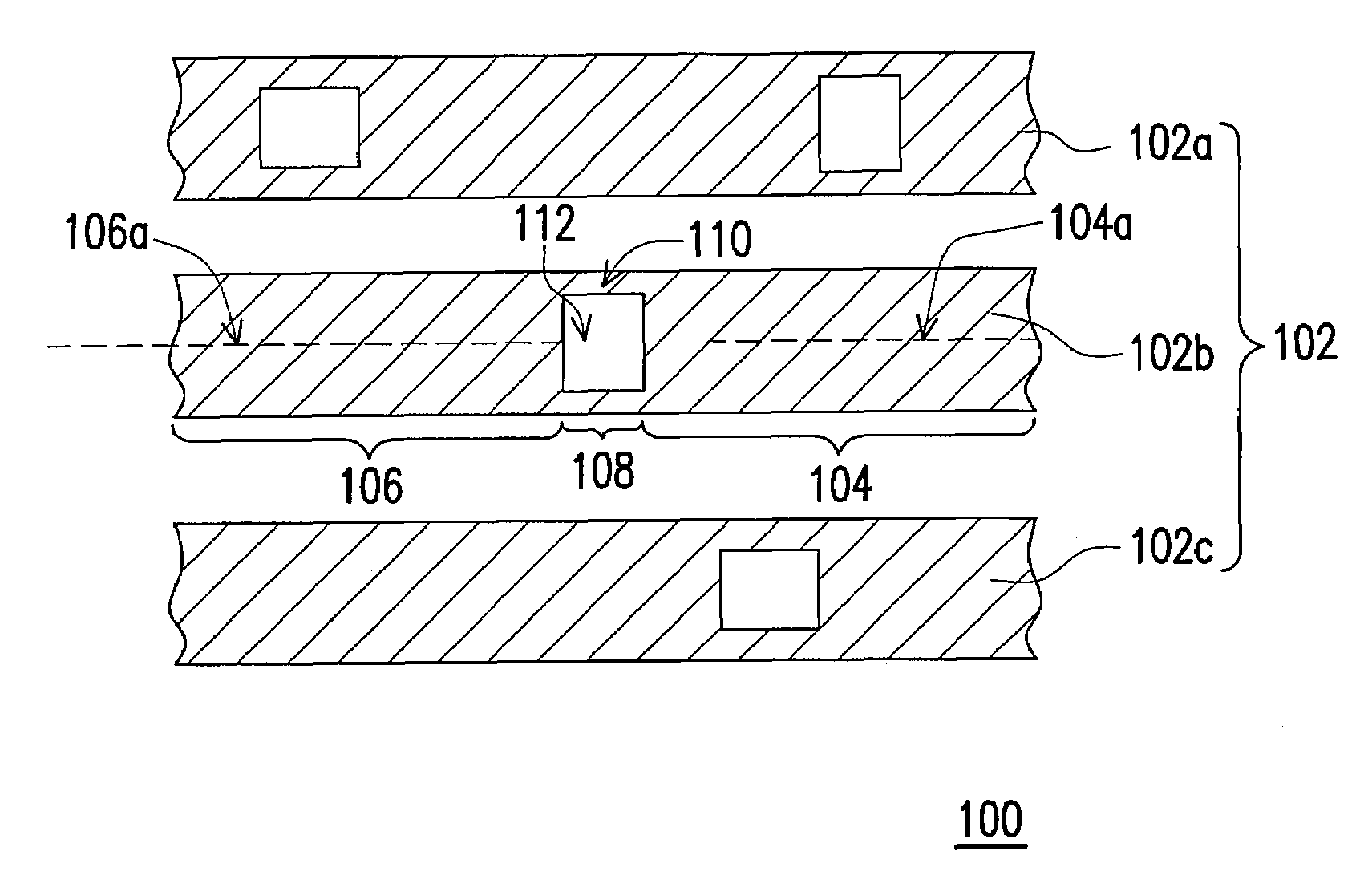
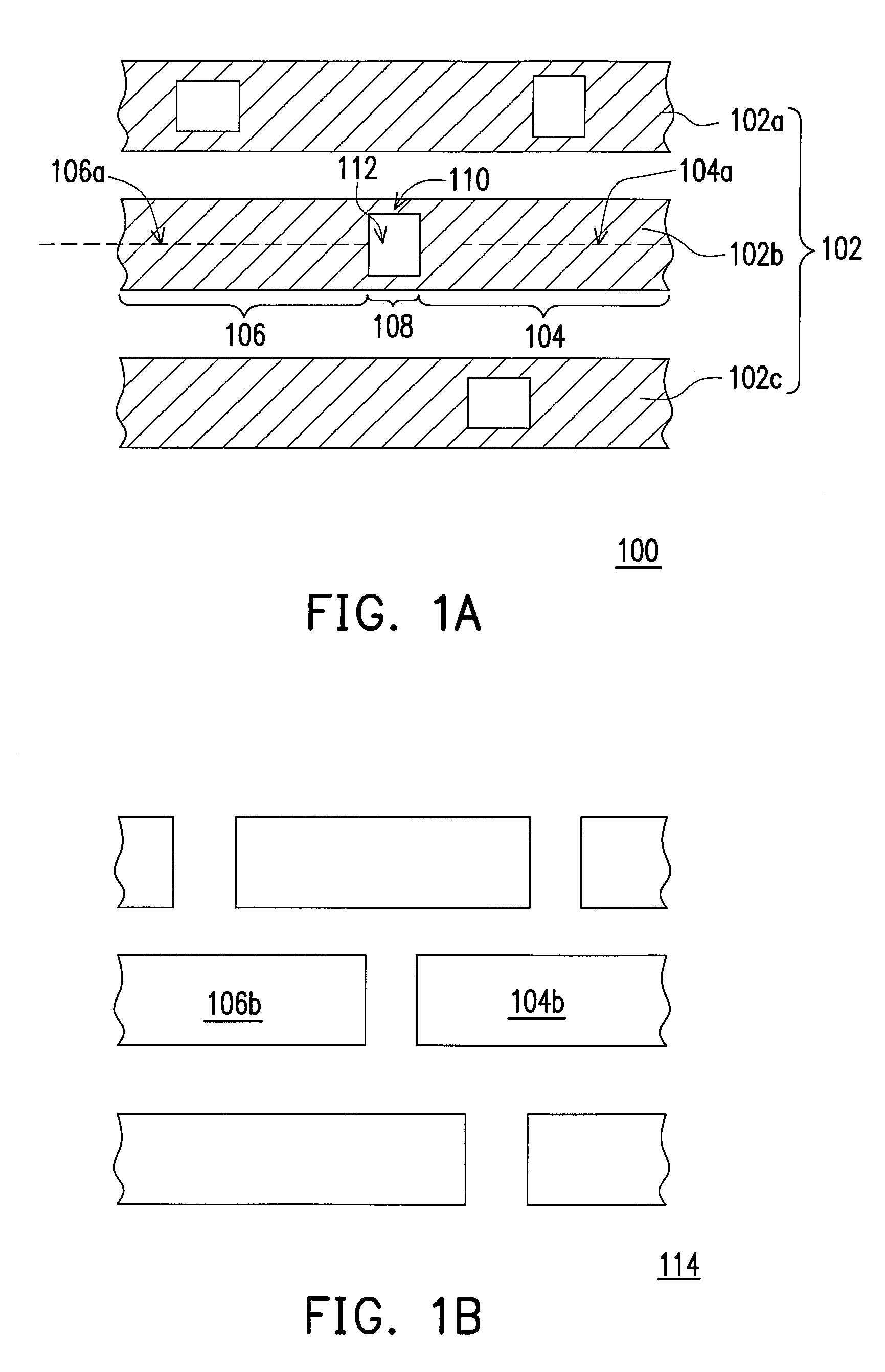
[0042]FIG. 1A is a schematic top view of a photo mask according to one embodiment of the present invention. As shown in FIG. 1A, a mask 100 has a mask pattern 102 thereon. The mask pattern 102 comprises at least one continuous pattern such as continuous patterns 102a, 102b and 102c. As the continuous pattern 102b shown in FIG. 1A, each of the continuous patterns possesses at least one connection region 108 which defines the continuous pattern 102b to be a first pattern 104 and a second pattern 106. The connection region 108 further comprises a closed opening 112 and a set of assistant patterns 110 through which the first pattern and the second pattern are connected to each other. In this embodiment, when the central axis 104a of the first pattern 104 is parallel to the central axis 106a of the second pattern 106, the assistant pattern 110 is located between the end of the first pattern 104 and the end of the second pattern 106. Hence, the set of the assistant pattern 110, the first ...


PUM

PropertyMeasurementUnit
dimensionaaaaaaaaaa
widthaaaaaaaaaa
sizeaaaaaaaaaa

Abstract

The invention provides a mask pattern. The mask pattern comprises at least a continuous pattern. Each of the continuous patterns has a first pattern, a second pattern and a set of assistance patterns. The assistant patterns are located between the first pattern to the second pattern. The first pattern, the assistant patterns and the second pattern together form a closed opening.

Description

BACKGROUND OF THE INVENTION[0001]1. Field of Invention[0002]The present invention relates to a mask pattern and method for forming the same. More particularly, the present invention relates to a mask pattern having a continuous pattern and method for forming the same.[0003]2. Description of Related Art[0004]As the integrated circuit is highly developed, the reduction and integration of the device become an inevitable tendency and are the main development task for the industry. In the manufacturing process of the integrated circuit, the photolithography process becomes a primary key for determining the device properties.[0005]With the increasing of the integration of the device, the size of the device is reduced and the distance between the devices is reduced as well. Therefore, the deviation occurs as the pattern is transferred from the mask to the material layer in the photolithography process. That is, when a pattern on a mask is transferred onto a wafer by using the photolithogra...

Claims


Application Information

Patent Timeline
Patent Type & Authority Patents(United States)
IPC IPC(8): G03F1/00
CPCG03F1/144G03F1/36
Inventor FU, CHUAN-HSIENYANG, CHUEN-HUEIKUO, CHIEN-LIWANG, SHU-RUWANG, YU-LIN
Owner UNITED MICROELECTRONICS CORP
Features
  • R&D
  • Intellectual Property
  • Life Sciences
  • Materials
  • Tech Scout
  • Unparalleled Data Quality
  • Higher Quality Content
  • 60% Fewer Hallucinations
Learn More