Check patentability & draft patents in minutes with Patsnap Eureka AI!

Foreign matter inspection apparatus

a technology for inspection apparatus and foreign matter, applied in the direction of material analysis, optically investigating flaws/contamination, instruments, etc., can solve the problems of insufficient alignment of wafers, adverse effects on inspection results, and inability to properly align wafers, so as to improve the inspection throughput of inspection apparatus and shorten the time

Inactive Publication Date: 2011-03-01
HITACHI HIGH-TECH CORP
View PDF12 Cites 0 Cited by
  • Summary
  • Abstract
  • Description
  • Claims
  • Application Information

AI Technical Summary

Benefits of technology

This solution enables high-precision alignment and detection of small foreign matters, reduces processing time, and enhances inspection throughput by automating the selection of suitable templates and alignment marks, even under challenging conditions.

Problems solved by technology

Because the difference signal is collected through comparison with the adjacent chips, variance occurs in the difference signal owing to the kind of the pattern contained in the detection region or the difference of the density such as wiring layout inside the chips and scribe lines among the chips and the inspection result is adversely affected.
Nonetheless, alignment has become more and more difficult owing to miniaturization of the alignment marks and the drop of contrast resulting from the manufacturing process.
However, immediately after the wafers are transferred to the stage, the wafers are not correctly aligned in the X and Y directions and must be positioned in the X and Y directions by rotating the stage.
However, the imaging visual field of the magnification camera is narrow and the probability of covering the correction marks by a single imaging operation becomes low.
However, this system involves the problem that alignment needs a long time.
However, the movement of the stage and the pattern matching processing become necessary and the processing time gets elongated.
This technology cannot be applied to a foreign matter inspection apparatus that requires high precision alignment of individual inspected objects.
Since the technology is directed to a reticle substrate produced as a jig that is dedicated to the adjustment of the positioning error, it does not take into consideration those adverse influences which may be exerted on various kinds of thin films produced in the manufacturing process of semiconductor devices such as semiconductor films, metal films, insulating films, and so forth, and problems of the recognition failure due to the drop of contrast of the alignment marks and the matching mistake with other alignment marks are unavoidable.
When an inspection process of semiconductor device products is a manufacturing process which invites the drop of contrast, however, it is difficult to observe the alignment marks with eye.
Therefore, the operator empirically repeats selection of the alignment marks but a long time is necessary to set a complicated evaluation condition of the template and a collection work.
Furthermore, when an error of an angle (θ) occurs in the inspected object, it is difficult to use the template as such and correction of the angle is necessary.
The error of the correction process results in the drop and variance of alignment accuracy.

Method used


Image

  • Foreign matter inspection apparatus
  • Foreign matter inspection apparatus
  • Foreign matter inspection apparatus

Examples


embodiment 1

[0053]FIG. 1 is a plan view showing a rough construction of a foreign matter inspection apparatus according to an embodiment of the invention. The foreign matter inspection apparatus includes one or more load ports 10, a transfer unit 20, a pre-alignment unit 30, an inspection unit 40 and a data processing unit 50. One or more wafer cassettes 11 accommodating a plurality of semiconductor wafers 1 to be inspected is put on the load ports 10. The wafer cassettes 11 may be divided into those for transferring the semiconductor wafers 1 to be inspected and those for recovering the semiconductor wafers 1 that are judged as defective as a result of inspection.

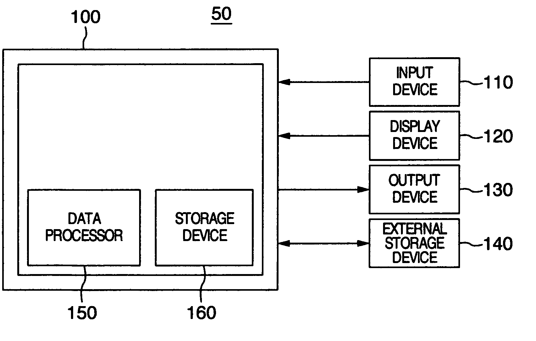
[0054]FIG. 2 is a block view showing an outline of control of the data processing unit 50. The data processing unit 50 includes a host computer 100, an input device 110 such as a keyboard, a touch panel or a mouse, a display device 120 such as a CRT or a flat panel display, an output device 130 such as a printer and an external storag...

embodiment 2

[0079]To discriminate the alignment marks by pattern matching, a template as a comparison object is necessary. Next, a method of collecting an optimal template from among the patterns formed on the semiconductor wafer 1 will be explained by mainly referring to FIGS. 6, 7 and 15. The explanation of those portions witch overlap with the first embodiment will be omitted and reference will be also made to FIGS. 1 and 2, whenever necessary.

[0080]FIG. 15 is a flowchart showing the processing procedure of the semiconductor wafer 1 in the second embodiment and FIG. 6 shows a CAD (Computer Aided Design) screen 720 for plotting a template candidate 710 of the alignment mark. The CAD screen 720 is provided as one of the functions of the foreign matter inspection apparatus and is displayed on the screen of the display device 120. The host computer 100 executes various processing for the CAD screen 720 on the basis of the instruction from the input device 110. A grid and a scale can be displayed...

embodiment 3

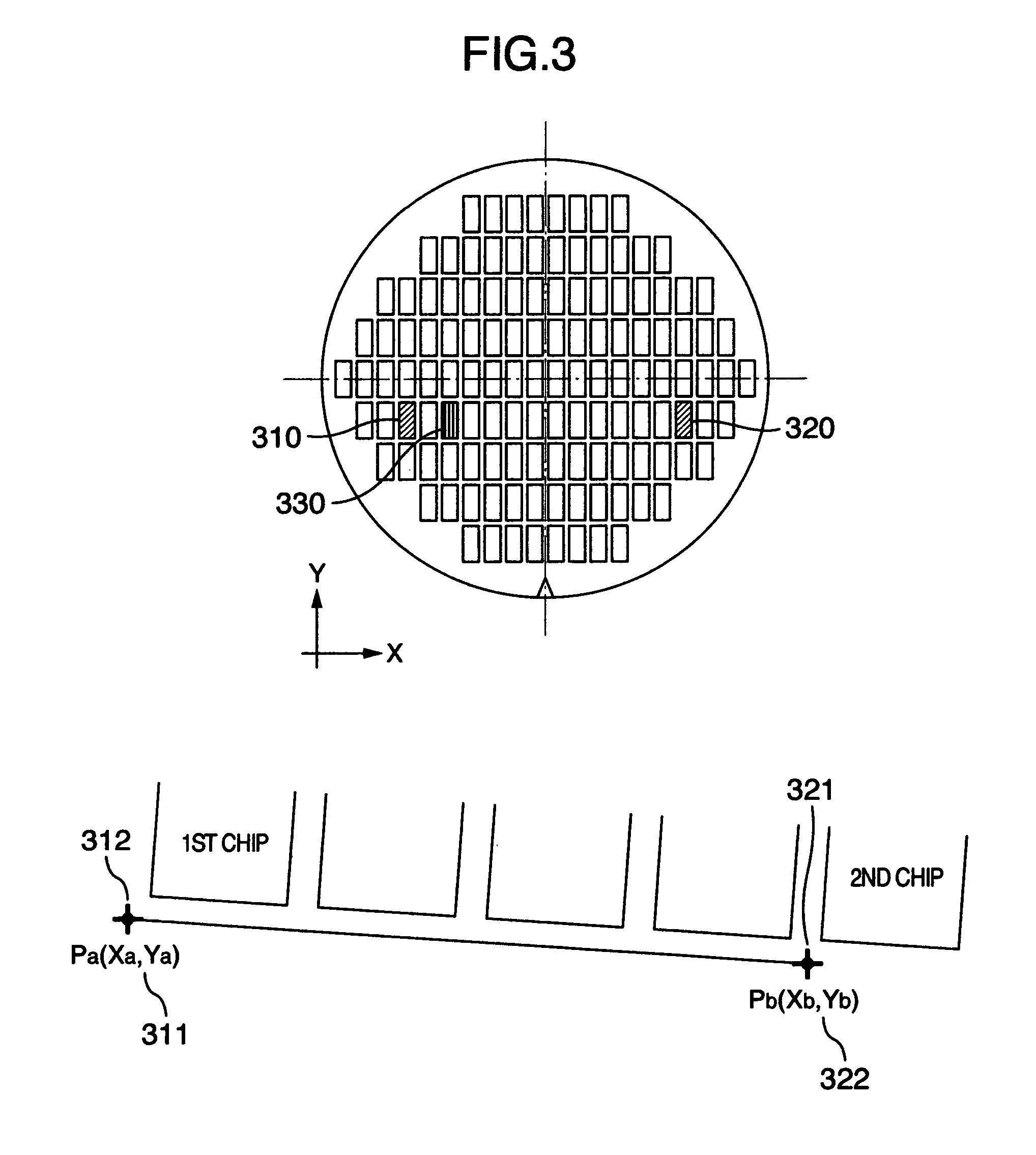
[0098]Next, a method for detecting the alignment marks formed on the semiconductor wafer 1 will be explained with primary reference to FIGS. 11, 12 and 16. However, the explanation of those portions which overlap with the first and second embodiments will be omitted and reference will be made also to FIGS. 1 and 2, whenever necessary.

[0099]FIG. 16 is a flowchart showing a processing procedure of the semiconductor wafer 1 in the third embodiment and FIG. 11 shows a set screen for detecting the alignment marks formed on the semiconductor wafer 1. The semiconductor wafer 1 as the measurement object is transferred by the wafer cassette 11 with the execution of the transfer program (S301) in the same way as in the first embodiment and is put on the inspection stage chuck 42 (S302 to S304). The inspection stage chuck 42 is then moved to the position of the designated chip 1210 in accordance with setting of the set screen (S305). After positioning is made to the designated coordinates 1220...


PUM

PropertyMeasurementUnit
contrasting-densityaaaaaaaaaa
thresholdaaaaaaaaaa
densityaaaaaaaaaa

Abstract

Selection with alignment marks of an optimal template, its identification and similarity judgment are conducted by a calculation function of a correlation value provided to a foreign matter inspection apparatus. In other words, the foreign matter inspection apparatus includes unit for registering feature points of alignment marks formed on a surface of an inspected object, unit for collecting image data of the alignment marks formed on the surface of the inspected object and a data processor for extracting a feature point from the image data and calculating a correlation value of both feature points, and registers the image data of the alignment mark on the basis of a threshold value of the correlation value.

Description

BACKGROUND OF THE INVENTION[0001]This invention relates to a foreign matter inspection apparatus for detecting foreign matters, scratches, defects, contamination, and so forth (which will be altogether referred to as “foreign matters”) existing on a surface of an inspected object such as a glass substrate, a semiconductor wafer, or the like. More particularly, the invention relates to a foreign matter inspection apparatus for highly precisely correcting a position of an inspected object and detecting foreign matters with high accuracy and high sensitivity.[0002]An apparatus for detecting the existence of foreign matters existing on a surface of an inspected object such as a glass substrate and a semiconductor wafer by irradiating an optical beam such as a laser beam to the surface of the inspected object and detecting a reflected or scattered beam occurring from the surface is known as a foreign matter inspection apparatus for (refer to JP-A-5-47901). In this foreign matter inspecti...

Claims


Application Information

Patent Timeline
Patent Type & Authority Patents(United States)
IPC IPC(8): G01N21/00
CPCG01N21/94G01N21/9501G01N21/95607
Inventor IMAI, EIJIOOYAMA, MASAMIOKAMOTO, HIDEYUKIYAMASHITA, HIROYUKI
Owner HITACHI HIGH-TECH CORP
Features
  • R&D
  • Intellectual Property
  • Life Sciences
  • Materials
  • Tech Scout
  • Unparalleled Data Quality
  • Higher Quality Content
  • 60% Fewer Hallucinations
Learn More