
Package on package using a bump-less build up layer (BBUL) package

a build-up layer and package technology, applied in the direction of semiconductor devices, semiconductor/solid-state device details, electrical equipment, etc., can solve the problem of creating to a prohibitively high z-heigh

Active Publication Date: 2012-01-10
INTEL CORP
View PDF56 Cites 64 Cited by
  • Summary
  • Abstract
  • Description
  • Claims
  • Application Information

AI Technical Summary

Problems solved by technology

One way to conserve space is to combine packages on top of packages, however this can create to a prohibitively high z-height as traditionally the top package would need to be elevated to clear the bottom package die.

Method used


Image

  • Package on package using a bump-less build up layer (BBUL) package
  • Package on package using a bump-less build up layer (BBUL) package
  • Package on package using a bump-less build up layer (BBUL) package

Examples


Embodiment Construction

[0009]In the following description, for purposes of explanation, numerous specific details are set forth in order to provide a thorough understanding of the invention. It will be apparent, however, to one skilled in the art that embodiments of the invention can be practiced without these specific details. In other instances, structures and devices are shown in block diagram form in order to avoid obscuring the invention.

[0010]Reference throughout this specification to “one embodiment” or “an embodiment” means that a particular feature, structure or characteristic described in connection with the embodiment is included in at least one embodiment of the present invention. Thus, appearances of the phrases “in one embodiment” or “in an embodiment” in various places throughout this specification are not necessarily all referring to the same embodiment. Furthermore, the particular features, structures or characteristics may be combined in any suitable manner in one or more embodiments.

[00...


PUM


Abstract

In some embodiments, package on package using a bump-less build up layer (BBUL) package is presented. In this regard, an apparatus is introduced comprising a microelectronic die having an active surface, an inactive surface parallel to said active surface, and at least one side, an encapsulation material adjacent said at least one microelectronic die side, wherein said encapsulation material includes a bottom surface substantially planar to said microelectronic die active surface and a top surface substantially planar to said microelectronic die inactive surface, a through via connection in said encapsulation material extending from said top surface to said bottom surface, a first dielectric material layer disposed on at least a portion of said microelectronic die active surface and said encapsulation material surface, a plurality of build-up layers disposed on said first dielectric material layer, and a plurality of conductive traces disposed on said first dielectric material layer and said build-up layers and in electrical contact with said microelectronic die active surface. Other embodiments are also disclosed and claimed.

Description

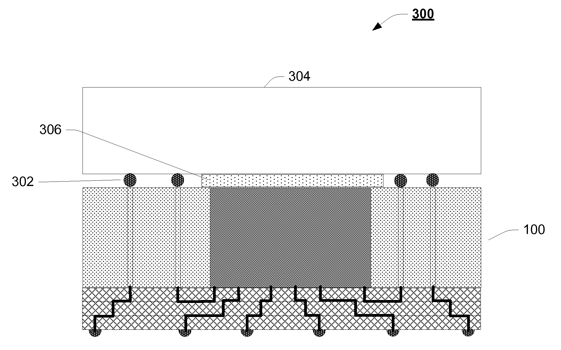
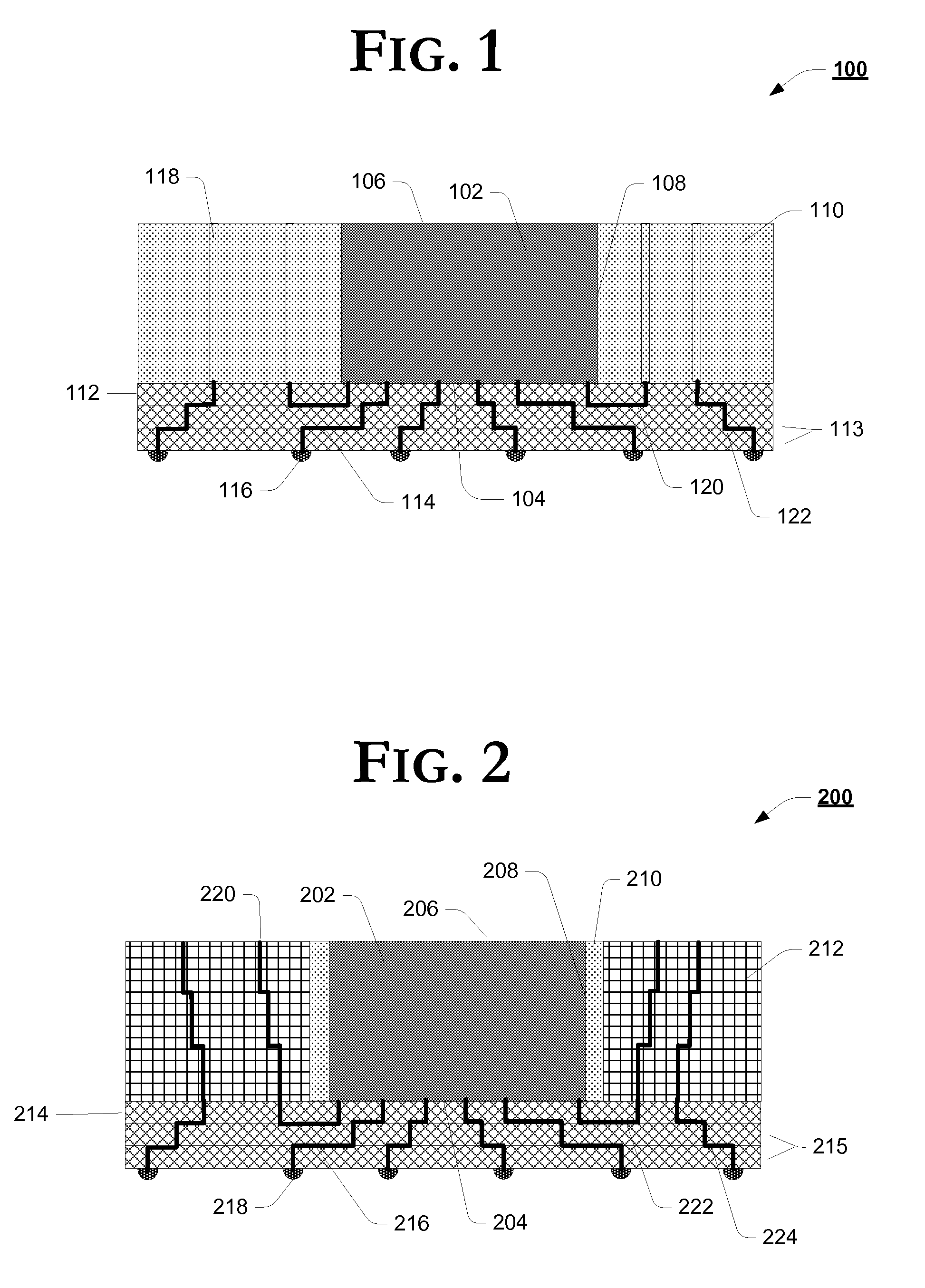
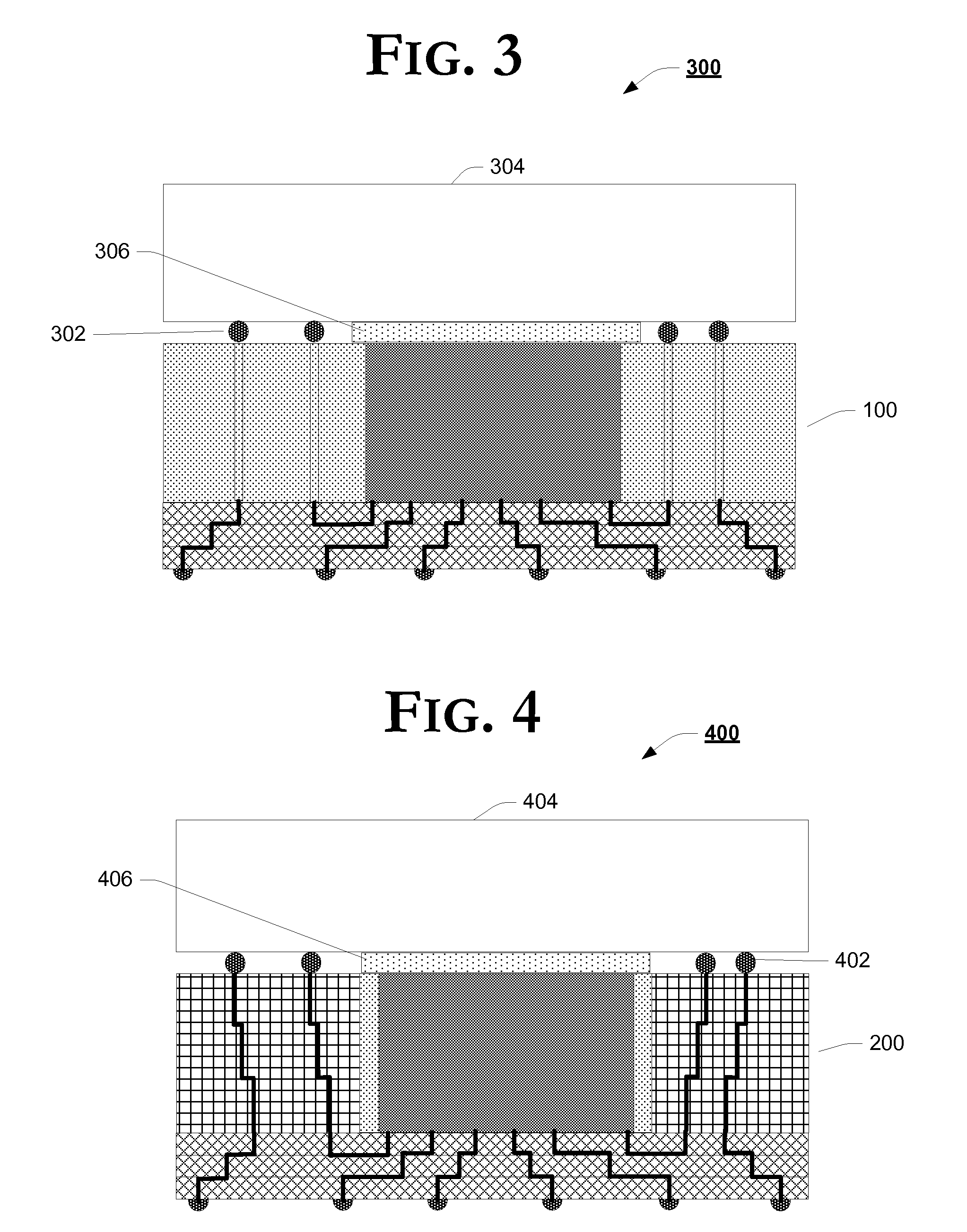
FIELD OF THE INVENTION[0001]Embodiments of the present invention generally relate to the field of integrated circuit package design and, more particularly, to package on package using a bump-less build up layer (BBUL) package.BACKGROUND OF THE INVENTION[0002]With shrinking electronic device sizes and increasing functionality, integrated circuit device packages will need to occupy less space. One way to conserve space is to combine packages on top of packages, however this can create to a prohibitively high z-height as traditionally the top package would need to be elevated to clear the bottom package die.BRIEF DESCRIPTION OF THE DRAWINGS[0003]The present invention is illustrated by way of example and not limitation in the figures of the accompanying drawings in which like references indicate similar elements, and in which:[0004]FIG. 1 is a graphical illustration of a cross-sectional view of a bump-less build up layer package, in accordance with one example embodiment of the inventio...

Claims


Application Information

Patent Timeline
Patent Type & Authority Patents(United States)
IPC IPC(8): H01L23/02
CPCH01L23/3157H01L23/5389H01L25/105H01L24/19H01L23/49822H01L2224/16235H01L23/49827H01L2224/16H01L2924/01078H01L2924/1433H01L2924/15311H01L2924/15331H01L2224/73204H01L2225/1023H01L2225/1058H01L2225/1094H01L2924/18162H01L2924/14H01L2924/00
Inventor PALMER, ERIC C.GUZEK, JOHN S.
Owner INTEL CORP
Learn More