
Apparatus and method for protecting fingerprint sensing circuitry from electrostatic discharge

a fingerprint sensing circuitry and electrostatic discharge technology, applied in electrostatic charges, instruments, computing, etc., can solve the problems of significant damage to internal components, increased risk of electrostatic discharge, and serious problems such as esd damag

Active Publication Date: 2012-01-31
SYNAPTICS INC
View PDF332 Cites 88 Cited by
  • Summary
  • Abstract
  • Description
  • Claims
  • Application Information

AI Technical Summary

Benefits of technology

The present invention provides an apparatus and method for dissipating electrostatic charge that accumulates on circuits such as fingerprint sensing circuits. This is achieved by applying an electrostatic discharge conductor to a non-conductive surface, which discharges the electrostatic charge resulting from a user swiping a fingerprint across the surface. This helps to protect sensitive circuits from electrostatic discharge and ensures reliable functioning of the apparatus.

Problems solved by technology

Electrostatic discharge (ESD) is a serious problem when dealing with many types of solid state electronics, such as integrated circuits (ICs), due to its ability to damage sensitive circuitry.
Contact between the body and a grounded IC can generate large enough currents through the IC to significantly damage internal components.
As transistors and other components of ICs continue to shrink in accordance with Moore's law, ESD damage becomes an even greater risk because of the smaller components' inability to withstand large currents.
The effects of ESD create special problems when dealing with electronics intended for touching by the body.
It would be infeasible as well as inconvenient for a user to have to ground his or her body prior to touching the sensor in order to dissipate an electrostatic charge.
Problems with ESD may be especially pronounced with conventional fingerprint sensors that allow a user to directly touch a piece of silicon.
Unfortunately, the fact that polyimide is a good insulator allows electrostatic charge to build up on the polyimide surface as a user swipes his or her finger.
In certain cases, the charge may discharge to the sensor circuitry, causing damage to sensitive electronic components such as IC I / O cells.

Method used


Image

  • Apparatus and method for protecting fingerprint sensing circuitry from electrostatic discharge
  • Apparatus and method for protecting fingerprint sensing circuitry from electrostatic discharge
  • Apparatus and method for protecting fingerprint sensing circuitry from electrostatic discharge

Examples


Embodiment Construction

[0020]It will be readily understood that the components of the present invention, as generally described and illustrated in the Figures herein, could be arranged and designed in a wide variety of different configurations. Thus, the following more detailed description of the embodiments of apparatus and methods in accordance with the present invention, as represented in the Figures, is not intended to limit the scope of the invention, as claimed, but is merely representative of certain examples of presently contemplated embodiments in accordance with the invention. The presently described embodiments will be best understood by reference to the drawings, wherein like parts are designated by like numerals throughout.

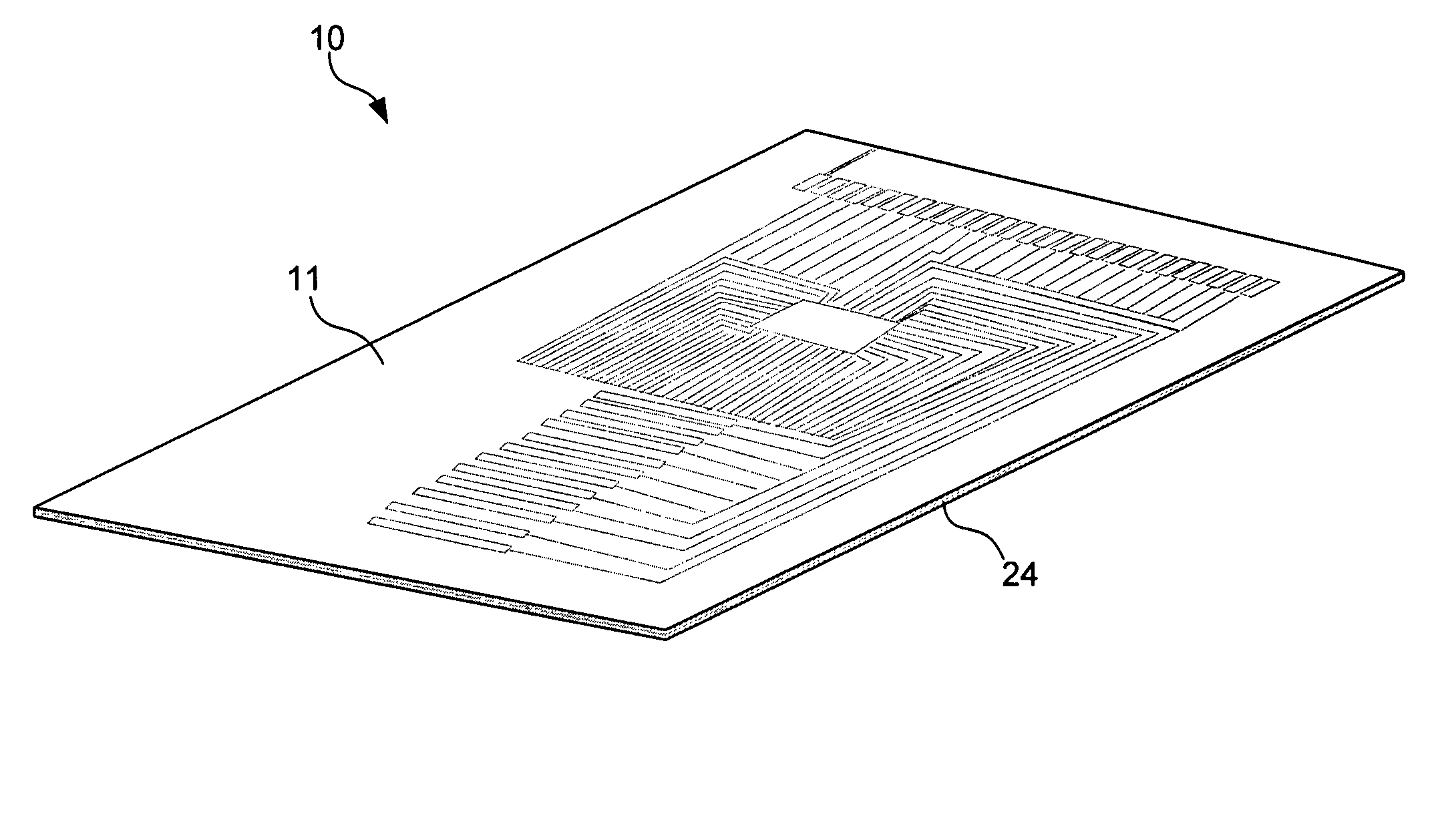
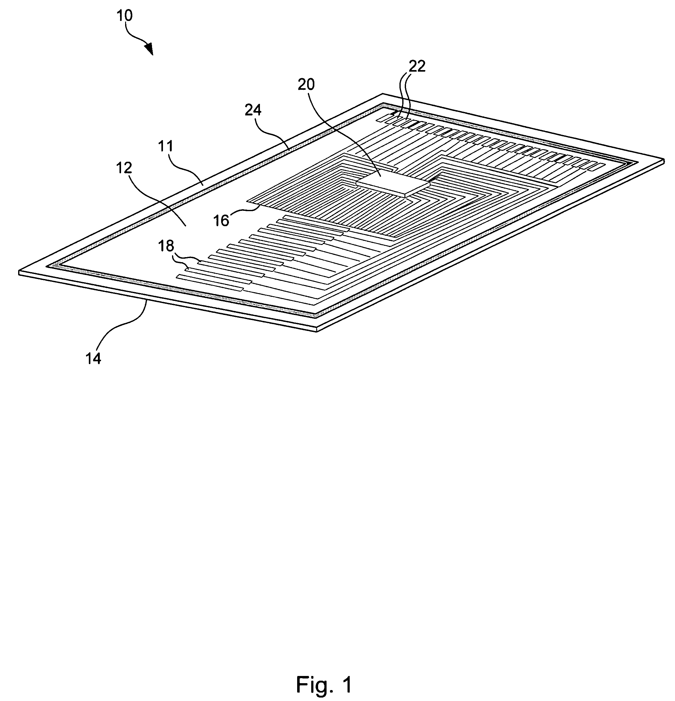
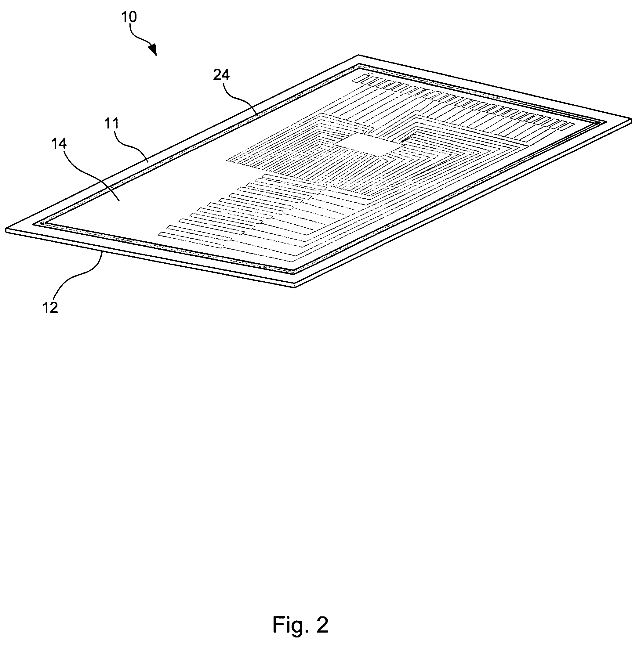
[0021]Referring to FIG. 1, a fingerprint sensing circuit 10 in accordance with a first embodiment of the invention may include a flexible non-conductive substrate 11 having a circuit side 12 and a sensing side 14. In certain embodiments, the substrate 11 may be constructed ...


PUM


Abstract

A fingerprint sensor in accordance with the invention includes a non-conductive substrate providing a first surface onto which a user can apply a fingerprint to be sensed. A sensor circuit is applied to a second surface of the non-conductive substrate opposite the first surface to sense a fingerprint when juxtaposed proximally thereto. An electrostatic discharge conductor is applied to the non-conductive surface and is located between an area where a fingerprint is swiped and the sensor circuit. The electrostatic discharge conductor discharges electrostatic charge resulting from a user swiping a fingerprint across the first surface.

Description

BACKGROUND OF THE INVENTION[0001]1. Field of the Invention[0002]This invention relates to electrostatic discharge (ESD) protection and more particularly to ESD protection for fingerprint sensing electronics.[0003]2. Description of the Related Art[0004]Electrostatic discharge (ESD) is a serious problem when dealing with many types of solid state electronics, such as integrated circuits (ICs), due to its ability to damage sensitive circuitry. Electronic components such as ICs may be exposed to ESD from various different sources, the most common of which is the human body. A body capacitance of approximately 150 pF can hold a charge of approximately 0.6 μC, which can generate potentials of several kV. Contact between the body and a grounded IC can generate large enough currents through the IC to significantly damage internal components.[0005]As transistors and other components of ICs continue to shrink in accordance with Moore's law, ESD damage becomes an even greater risk because of t...

Claims


Application Information

Patent Timeline
Patent Type & Authority Patents(United States)
IPC IPC(8): H01H47/00H05F3/02
CPCG06K9/00053G06V40/1329
Inventor NELSON, RICHARD BRIANERHART, RICHARD ALEXANDERPEREZSELSKY, ARMANDO LEON
Owner SYNAPTICS INC
Learn More