Substrate processing apparatus and attaching/detaching method of reaction vessel

a technology of substrate processing and reaction vessel, which is applied in the direction of lighting and heating apparatus, manufacturing tools, furniture, etc., can solve the problems of time-consuming maintenance work and difficult installation of reaction vessel

Active Publication Date: 2012-05-08
KOKUSA ELECTRIC CO LTD
View PDF7 Cites 329 Cited by
  • Summary
  • Abstract
  • Description
  • Claims
  • Application Information

AI Technical Summary

Benefits of technology

[0017]An object of the present invention is to provide a substrate processing apparatus capable of performing maintenance of a reaction vessel without changing a device height or without changing a reaction vessel size, and an attaching / detaching method of the reaction vessel.
[0024]According to the present invention, the maintenance of the reaction vessel can be performed without changing a device height and without changing a reaction vessel size.

Problems solved by technology

Therefore, it becomes difficult to install the reaction vessel 307 in the heater unit 306.
Accordingly, a structure of the attachment / detachment jig 300 is complicated, thus generating a time-consuming maintenance work.

Method used


Image

  • Substrate processing apparatus and attaching/detaching method of reaction vessel
  • Substrate processing apparatus and attaching/detaching method of reaction vessel
  • Substrate processing apparatus and attaching/detaching method of reaction vessel

Examples


Embodiment Construction

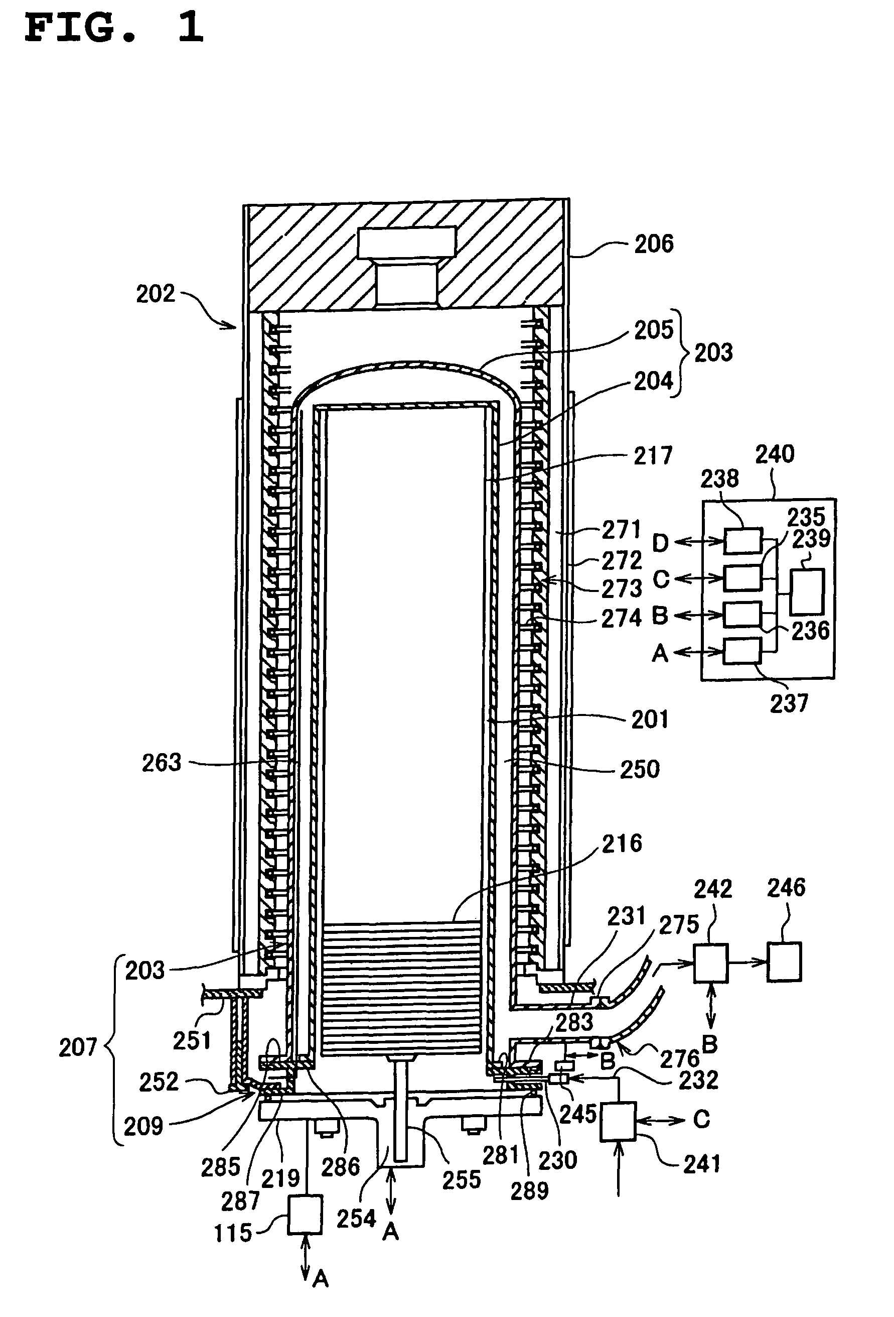
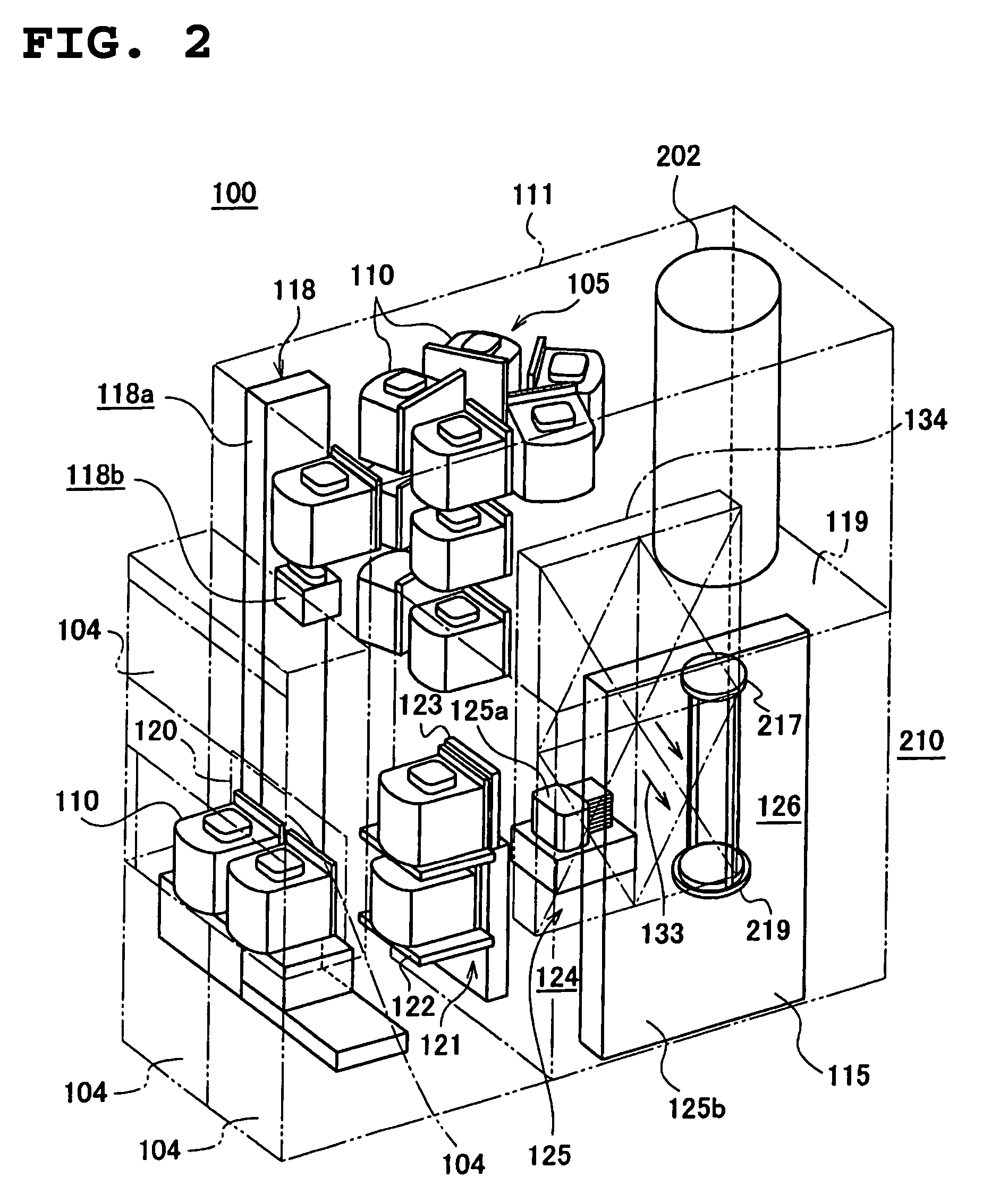
[0047]According to a preferred embodiment for executing the present invention, the substrate processing apparatus is constituted as a semiconductor manufacturing apparatus to execute a processing step in a manufacturing method of a semiconductor device (IC), as an example. Note that hereunder, an explanation is given to a case that the substrate processing apparatus of the present invention is applied to a vertical semiconductor manufacturing device (called simply a processing apparatus hereunder) as a semiconductor manufacturing device, for performing oxidation, diffusion processing and a CVD processing. FIG. 2 shows a perspective view of the processing apparatus applied to an embodiment of the present invention. In addition, FIG. 3 is a side perspective view of the processing apparatus shown in FIG. 2.

[0048]As is shown in FIG. 2 and FIG. 3, a casing 111 is included in a processing apparatus 100 of this embodiment, in which hoops (substrate containers, called pods hereunder) 110 ar...


PUM

PropertyMeasurementUnit
weightaaaaaaaaaa
thicknessaaaaaaaaaa
heat resistanceaaaaaaaaaa

Abstract

To provide a substrate processing apparatus, comprising: a reaction vessel having a processing chamber inside that processes a substrate; a heating device that heats said substrate from an outer peripheral side of the reaction vessel; a lid member that closes the processing chamber; an attachment / detachment jig placed on the lid member for attaching / detaching the reaction vessel from an inside of the heating device; and a support section provided in an upper side of a lower end of the reaction vessel on an inside wall of the reaction vessel, and abutted on an upper surface of the attachment / detachment jig for attaching / detaching the reaction vessel from the inside of the heating device.

Description

BACKGROUND[0001]1. Technical Field[0002]The present invention relates to a substrate processing apparatus and an attaching / detaching method of a reaction vessel, and for example relates to the substrate processing apparatus used in a semiconductor manufacturing apparatus and an attaching / detaching method of the reaction vessel.[0003]2. Background Art[0004]FIG. 20 shows a sectional view of a batch type vertical processing furnace that simultaneously processes a plurality of wafers used in a conventional substrate processing apparatus.[0005]A vertical processing furnace 302 is provided in a casing not shown. This vertical processing furnace 302 is composed of a heater unit 306 and a reaction vessel 307 inserted into the heater unit 306. The reaction vessel 307 is composed of a reaction tube 303 and a furnace throat flange 309 for supporting the reaction tube 303. The reaction tube 303 is composed of an outer tube 305 and an inner tube 304 provided in the outer tube 305. The furnace th...

Claims


Application Information

Patent Timeline
Patent Type & Authority Patents(United States)
IPC IPC(8): C23C16/00C23C16/44C23C16/46F27D1/18F28D21/00H01L21/31H01L21/22H01L21/205B21D39/00B01J19/00H01L21/00H01L21/02
CPCH01L21/67126H01L21/67757Y10T29/49Y10T29/4981Y10T29/49799Y10T29/49826H01L21/02H01L21/00
Inventor SHIBATA, KOJITATTA, MASAHIRO
Owner KOKUSA ELECTRIC CO LTD
Why Eureka
Try Eureka