Signal analyzing method for electronic device having on-chip network and off-chip network

a technology of electronic devices and signals, applied in the field of signal analysis methods, can solve the problems of inability to provide accurate phases of signals, inability of analysis methods to provide complete electrical connections inability to provide accurate electrical characteristics between two different interfaces, etc., to achieve accurate electrical characteristics

Inactive Publication Date: 2012-06-19
HIMAX TECH LTD
View PDF7 Cites 0 Cited by
  • Summary
  • Abstract
  • Description
  • Claims
  • Application Information

AI Technical Summary

Benefits of technology

[0014]Compared with the conventional signal analyzing method for an electronic device having an on-chip network and an off-chip network, the signal analyzing method disclosed by the present invention is able to provide a complete electrical connection and accurate electrical characteristics for an electronic device having an on-chip network and an off-chip network.

Problems solved by technology

However, this conventional signal analyzing method is not able to provide accurate electrical characteristics between two different interfaces, because when the method analyzes signals at high frequency, the phases of the signals are not accurate.
However, this conventional signal analyzing method is not able to provide a complete electrical connection between two different interfaces.

Method used


Image

  • Signal analyzing method for electronic device having on-chip network and off-chip network
  • Signal analyzing method for electronic device having on-chip network and off-chip network
  • Signal analyzing method for electronic device having on-chip network and off-chip network

Examples


Embodiment Construction

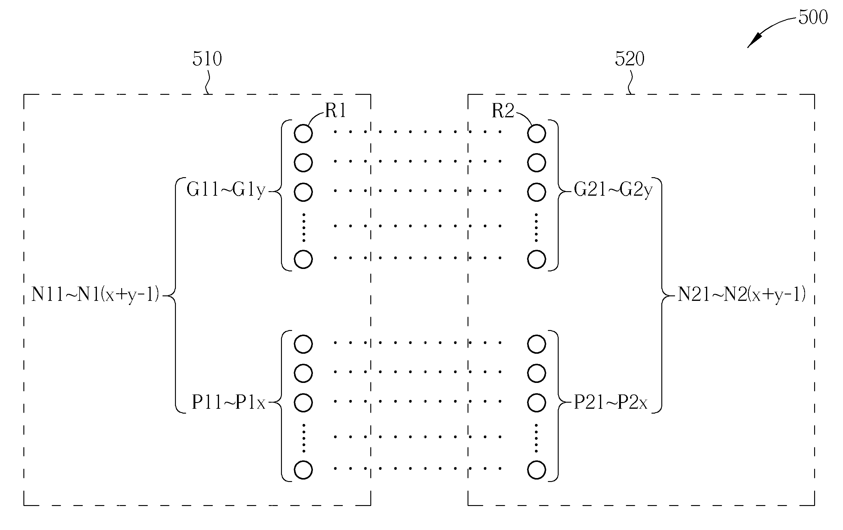
[0022]Please refer to FIG. 5 and FIG. 6. FIG. 5 shows a simplified diagram of an electronic device 500 having an on-chip network 510 and an off-chip network 520 in accordance with an embodiment of the present invention. The on-chip network 510 can be an integrated circuit (IC), and the off-chip network can be a circuit board 520. FIG. 6 shows a flowchart of a signal analyzing method for the electronic device 500. As shown in FIG. 5 and FIG. 6, the signal analyzing method comprises:

[0023]Step 600: Define a number X of first power nodes P11˜P1x and a number Y of first ground nodes G11˜G1y in the on-chip network 510, wherein X and Y are positive integers.

[0024]Step 610: Define a number X of second power nodes P21˜P2x and a number Y of second ground nodes G21˜G2y in the off-chip network 520.

[0025]Step 620: Assign one of the first ground nodes G11˜G1y as a first reference node R1.

[0026]Step 630: Assign one of the second ground nodes G21˜G2y as a second reference node R2.

[0027]Step 640: U...


PUM


Abstract

The present invention provides a signal analyzing method for an electronic device having an on-chip network and an off-chip network. Compared with the conventional signal analyzing method for an electronic device having an on-chip network and an off-chip network, the signal analyzing method of the present invention is able to provide a complete electrical connection and accurate electrical characteristics for an electronic device having an on-chip network and an off-chip network.

Description

BACKGROUND OF THE INVENTION[0001]1. Field of the Invention[0002]The present invention relates to a signal analyzing method, and more particularly, to a signal analyzing method for an electronic device having an on-chip network and an off-chip network.[0003]2. Description of the Prior Art[0004]Please refer to FIG. 1 and FIG. 2. FIG. 1 shows a simplified diagram of a conventional electronic device 100 having an on-chip network 110 and an off-chip network 120. FIG. 2 shows a flowchart of a conventional signal analyzing method for the electronic device 100. As shown in FIG. 1 and FIG. 2, the conventional signal analyzing method comprises the following steps:[0005]Step 200: Define a number X of first power nodes P11˜P1x and a number Y of first ground nodes G11˜G1y in the on-chip network 110.[0006]Step 210: Define a number X of second power nodes P21˜P2x and a number Y of second ground nodes G21˜G2y in the off-chip network 120.[0007]Step 220: Utilize a quasi-static electromagnetic simulat...

Claims


Application Information

Patent Timeline
Patent Type & Authority Patents(United States)
IPC IPC(8): G06F17/50
CPCG06F17/5036G06F30/367
Inventor HSU, HSING-CHOUCHEN, TUNG-YANG
Owner HIMAX TECH LTD
Why Eureka
Try Eureka