Signal analyzing method for electronic device having on-chip network and off-chip network
- Summary
- Abstract
- Description
- Claims
- Application Information
AI Technical Summary
Benefits of technology
Problems solved by technology
Method used
Image

Examples
Embodiment Construction
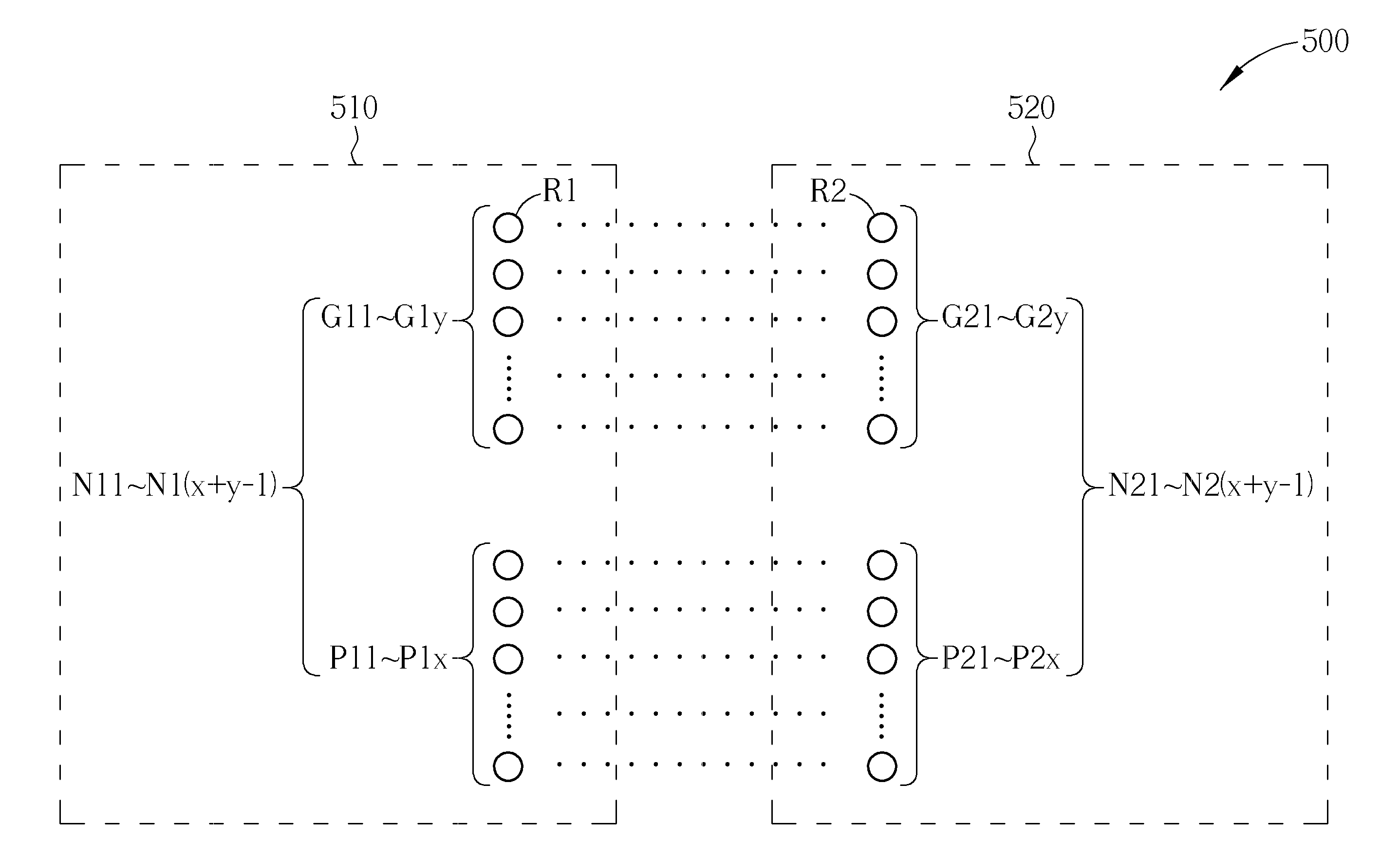
[0022]Please refer to FIG. 5 and FIG. 6. FIG. 5 shows a simplified diagram of an electronic device 500 having an on-chip network 510 and an off-chip network 520 in accordance with an embodiment of the present invention. The on-chip network 510 can be an integrated circuit (IC), and the off-chip network can be a circuit board 520. FIG. 6 shows a flowchart of a signal analyzing method for the electronic device 500. As shown in FIG. 5 and FIG. 6, the signal analyzing method comprises:
[0023]Step 600: Define a number X of first power nodes P11˜P1x and a number Y of first ground nodes G11˜G1y in the on-chip network 510, wherein X and Y are positive integers.
[0024]Step 610: Define a number X of second power nodes P21˜P2x and a number Y of second ground nodes G21˜G2y in the off-chip network 520.
[0025]Step 620: Assign one of the first ground nodes G11˜G1y as a first reference node R1.
[0026]Step 630: Assign one of the second ground nodes G21˜G2y as a second reference node R2.
[0027]Step 640: U...
PUM
 Abstract
Description
Claims
Application Information
 - R&D Engineer
- R&D Manager
- IP Professional
- Industry Leading Data Capabilities
- Powerful AI technology
- Patent DNA Extraction
Browse by: Latest US Patents, China's latest patents, Technical Efficacy Thesaurus, Application Domain, Technology Topic.
© 2024 PatSnap. All rights reserved.Legal|Privacy policy|Modern Slavery Act Transparency Statement|Sitemap