

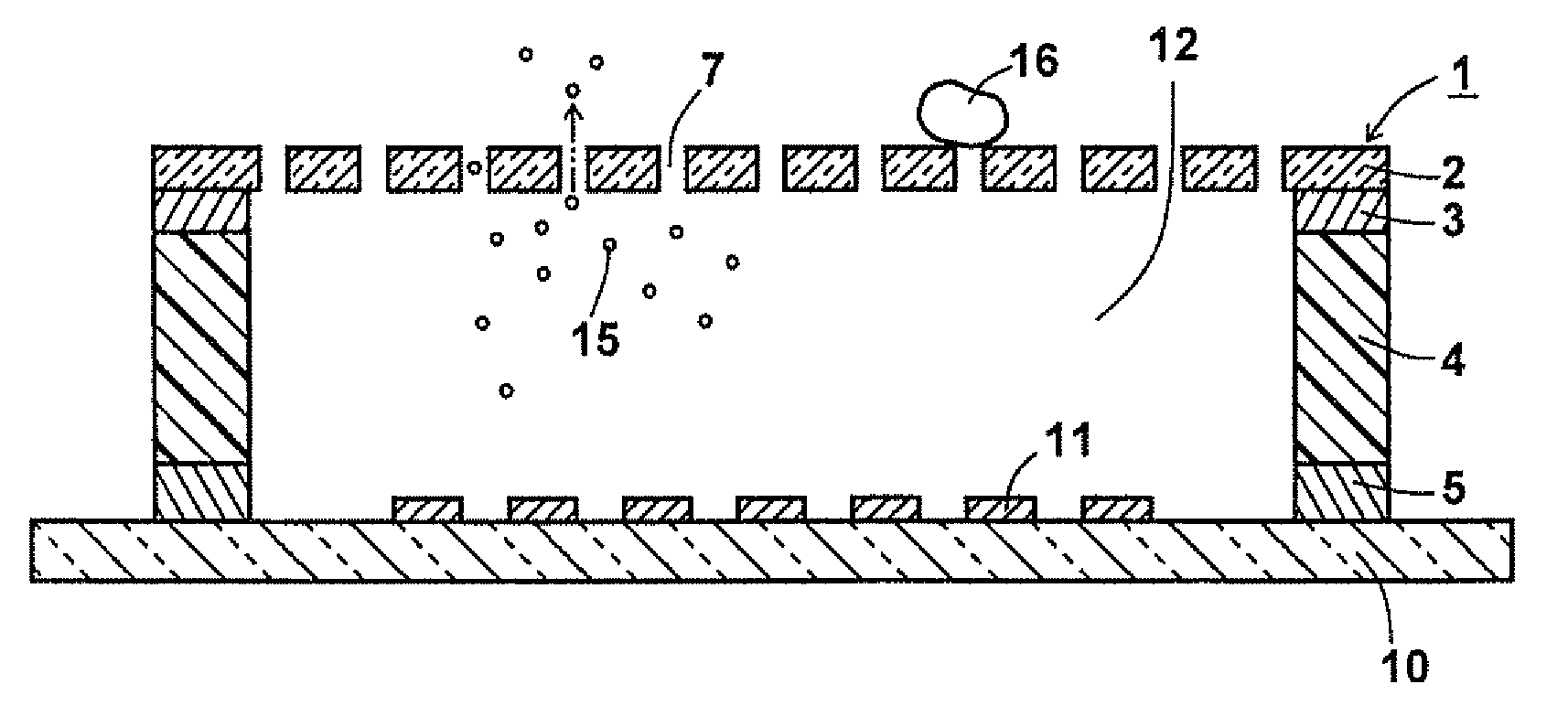
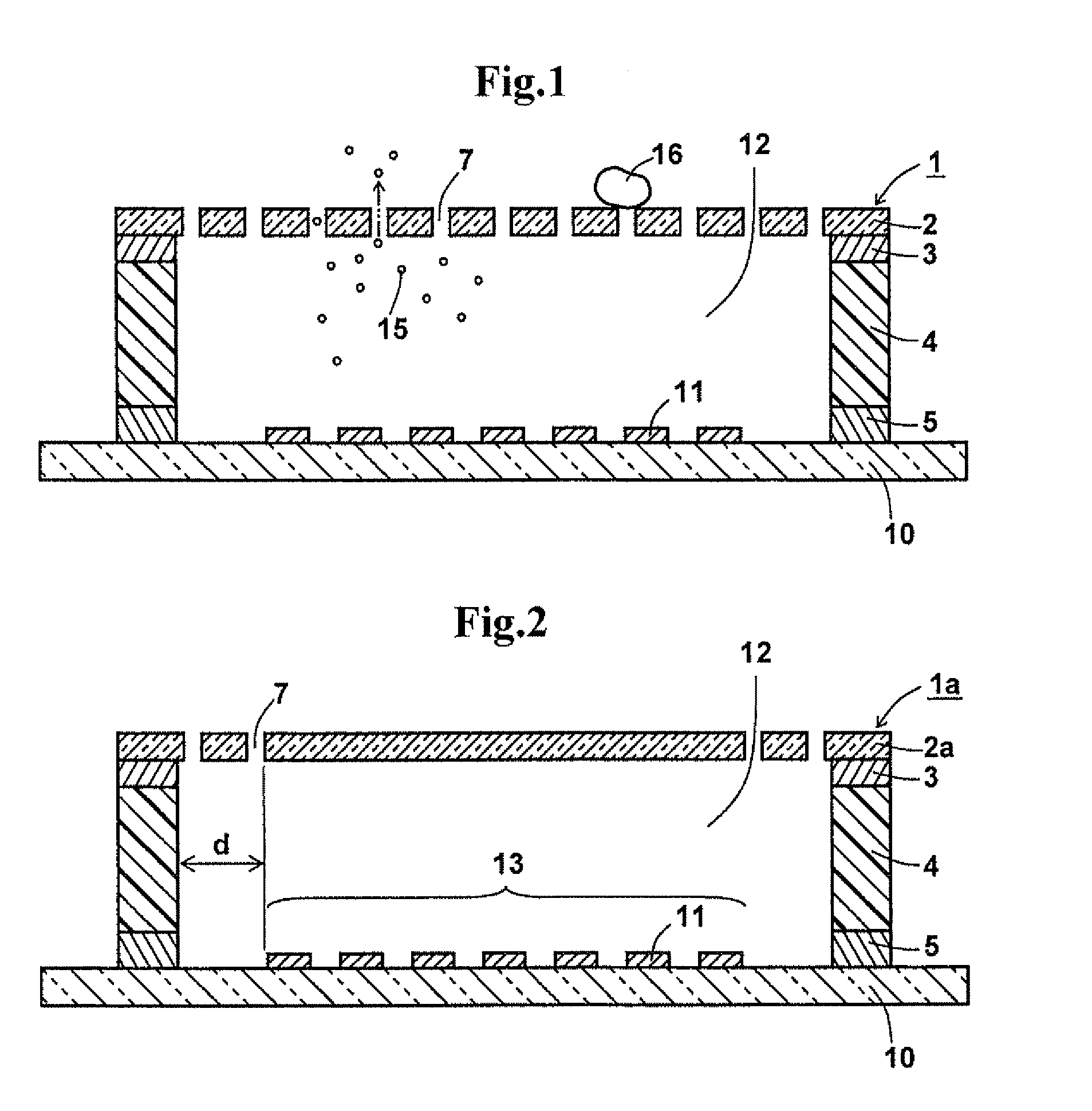
Pellicle for lithography and method for manufacturing pellicle film
a technology which is applied in the field of lithography and pellicle film manufacturing, can solve the problems of minute foreign particles such as dust, deformation and disconnection of circuit patterns, rough edges of circuit patterns, etc., and achieve the effect of highly precise and easy formation
- Summary
- Abstract
- Description
- Claims
- Application Information
AI Technical Summary
Benefits of technology
Problems solved by technology
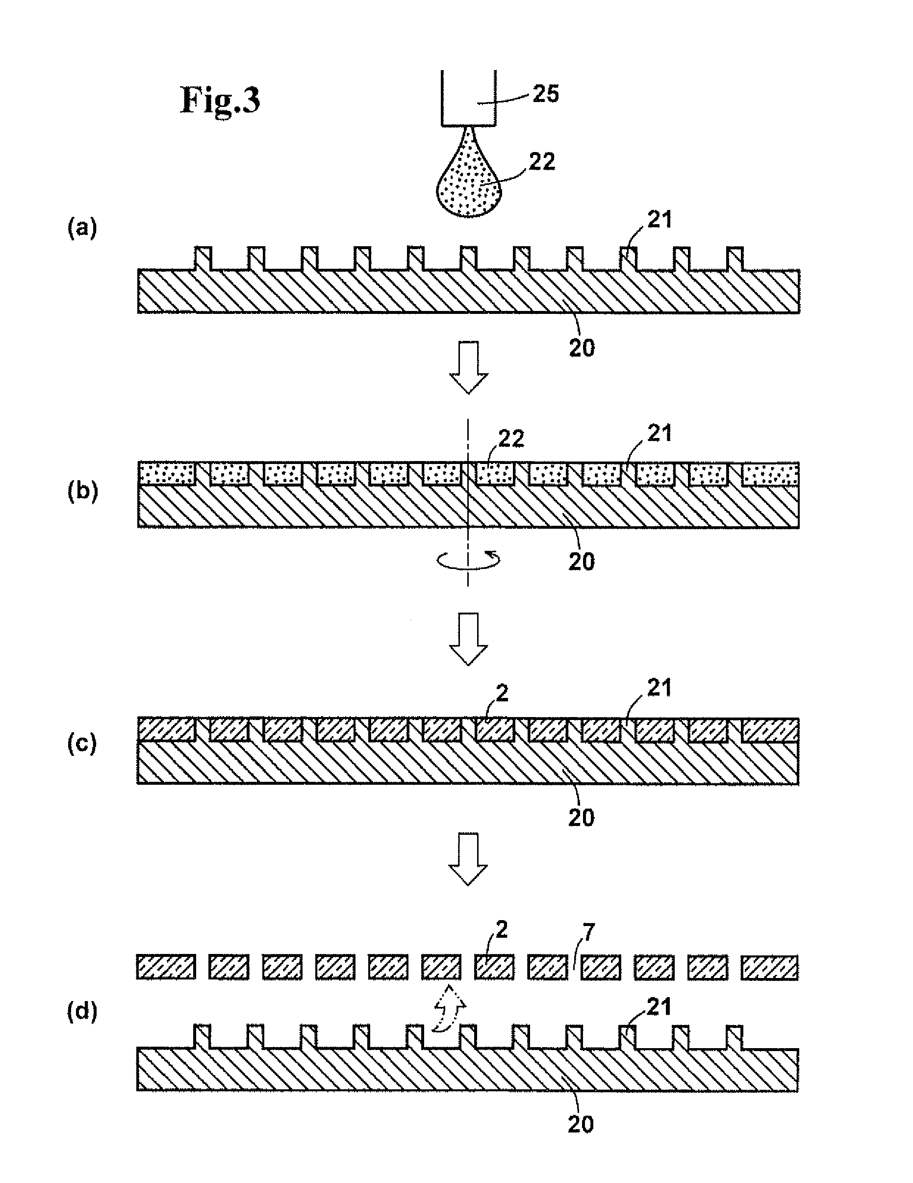
Method used
Image

Examples
example 2
[0078]A silicon wafer having the diameter of 300 mmØ was used as an original plate material for the film-forming substrate. A resist film was formed by coating the surface of the wafer with the resist liquid. Exposure was carried out at the reduction rate of 1 / 4 using a mask (150 mm-square) having holes measuring 0.2 μm in diameter formed all over the surface thereof. The mask was moved on the wafer so that the whole surface of the wafer was exposed to light. The resist was developed to leave the exposed portion. And then etching was carried out to form a concave-convex shape on the silicon wafer. Finally, the resist was removed, and then the wafer was cleaned. Thus a substrate for pellicle-film formation was prepared. The diameter of the convex portion on the wafer surface was 0.05 μm and the height of the step was 0.3 μm. The density of the convex portion was 0.01 mm2 per 1 mm2.
[0079]On the central portion of this film-forming substrate (silicon wafer), the 3% solution of “Cytop C...
example 3
[0082]A silicon wafer having the diameter of 300 mmØ was used as an original plate material for the film-forming substrate. A resist film was formed by coating the surface of the wafer with the resist liquid. Exposure was carried out at the reduction rate of 1 / 4 using a mask having holes measuring 0.4 μm in diameter formed all over the surface thereof. The mask was moved on the wafer so that a region other than the wafer's central portion (105 mm×69 mm) was exposed to light. The resist was developed to leave the exposed portion. And then etching was carried out to form a concave-convex shape on the silicon wafer. Finally, the resist was removed and then the wafer was cleaned. Thus a substrate for pellicle-film formation was prepared. The diameter of the convex portion on a wafer surface of the portion other than the_wafer's central portion (105 mm×69 mm) was 0.1 μm, and the height of the step of the convex portion was 0.3 μm. The density of the convex portion was 0.5 mm2 per 1 mm2.
[...
example 4
[0089]A silicon wafer having the diameter of 300 mmØ was used as an original plate material for the film-forming substrate. A resist film was formed by coating the surface of the wafer with the resist liquid. Exposure was carried out at the reduction rate of 1 / 4 using a mask having holes measuring 0.4 μm in diameter formed all over the surface thereof. The mask was moved on the wafer so that a portion other than the wafer's central portion (135 mm×99 mm) was exposed to light. The resist was developed to leave only the exposed portion. And then etching was carried out to form concave-convex shape on the silicon wafer. Finally, the resist was removed and then the wafer was cleaned. Thus the substrate for pellicle-film formation was prepared. The diameter of the convex portion on the wafer surface in the region other than the_wafer's central portion (135 mm×99 mm) was 0.1 μm and the height of the step of the convex portion was 0.3 μm. The density of the convex portion was 0.5 mm2 per 1...
PUM
| Property | Measurement | Unit |
|---|---|---|
| diameter | aaaaa | aaaaa |
| size | aaaaa | aaaaa |
| particle size | aaaaa | aaaaa |
Abstract
Description
Claims
Application Information