Pellicle for lithography and method for manufacturing pellicle film

a technology of lithography and pellicle film, which is applied in the field of lithography pellicle and lithography manufacturing pellicle film, can solve the problems of minute foreign particles such as dust, deformation and disconnection of circuit patterns, rough edges of circuit patterns, etc., and achieves fast gas discharge, high precision and easy formation, and fast gas discharge

Active Publication Date: 2011-08-25
SHIN ETSU CHEM IND CO LTD
View PDF2 Cites 8 Cited by
  • Summary
  • Abstract
  • Description
  • Claims
  • Application Information

AI Technical Summary

Benefits of technology

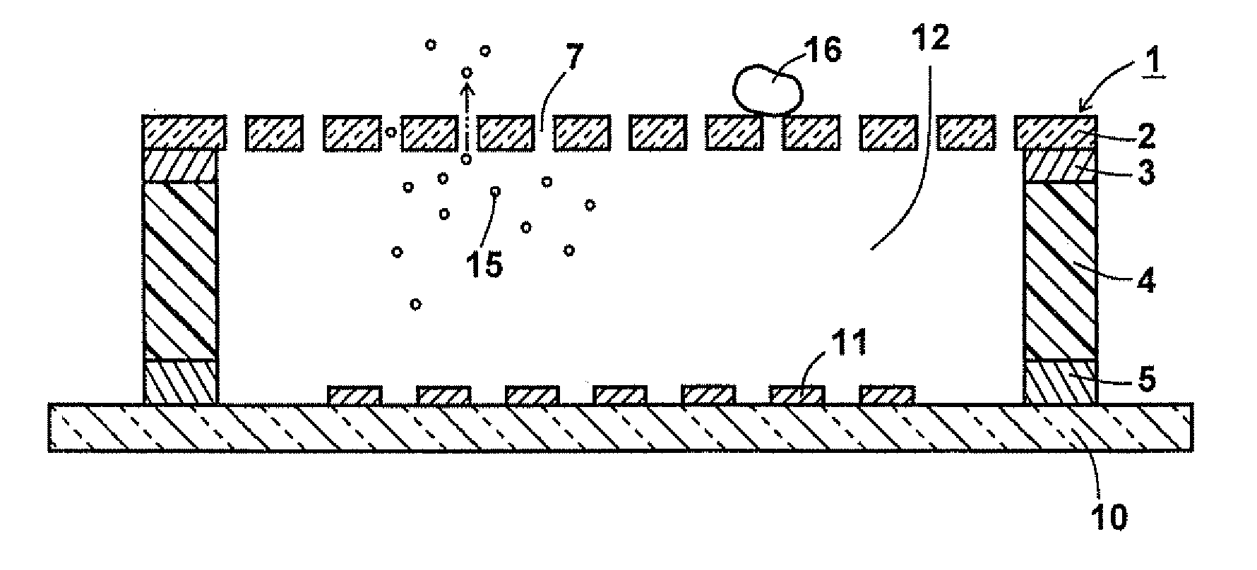
The present invention was made to solve the problems described above and an object of the present invention is to provide a pellicle for lithography which can prevent a haze from generating on a photomask even if a short-wave laser beam such as an ArF excimer laser beam is used for a long period of time. Another object of the present invention is to provide a method for manufacturing a pellicle film to be attached to the pellicle for lithography.
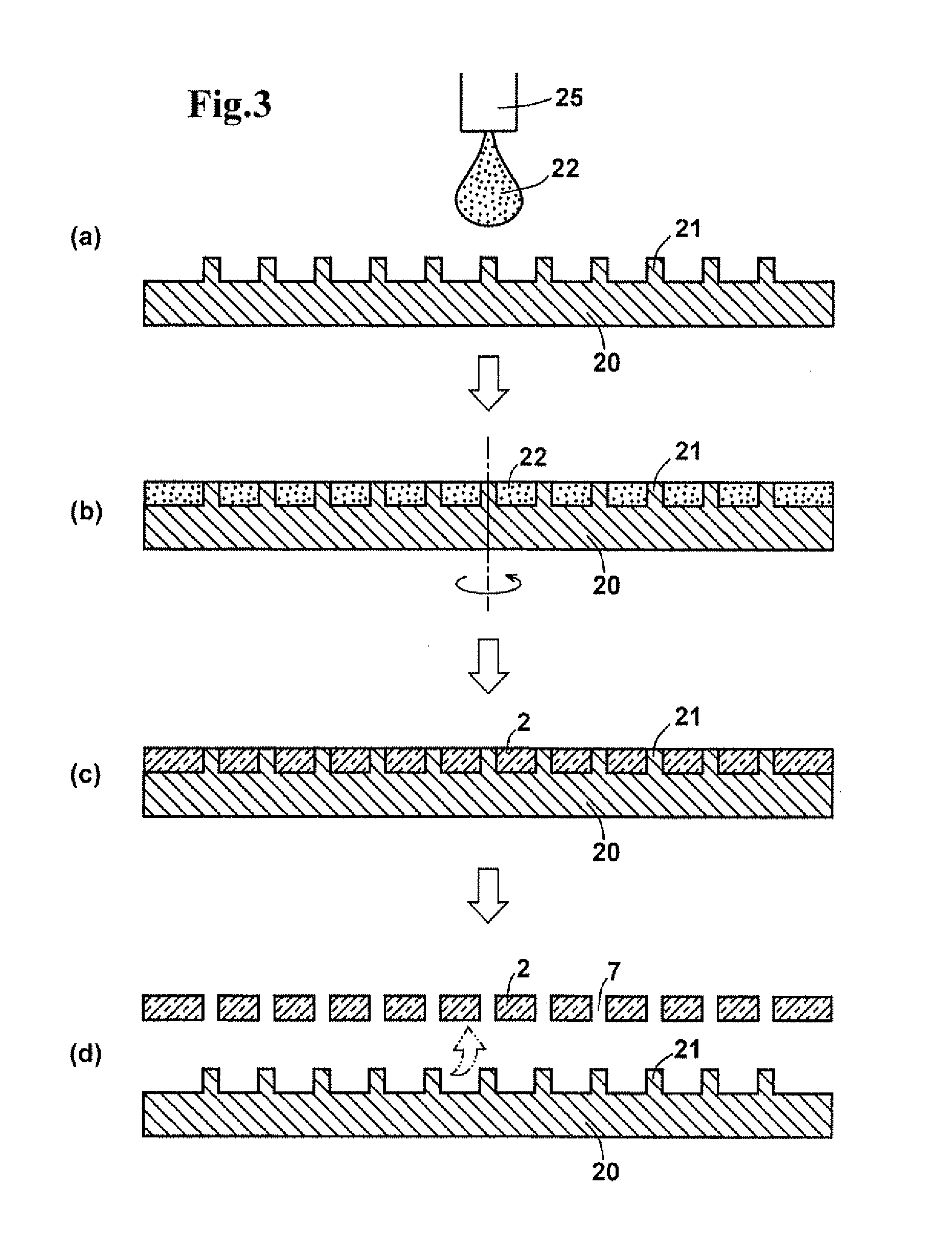
According to the method for producing the pellicle film, film formation is carried out by a spin coating method using a film-forming substrate having a convex portion whose size fits into the venting hole. A minute venting hole can be formed highly precisely and easily.

Problems solved by technology

Formation of the circuit pattern using this lithographic technology is usually carried out in a clean room, but even in the clean room there are minute foreign particles such as dust.
If the foreign particle adheres to the photomask, the particle causes reflection, shading and scattering of light, and therefore deformation and disconnection of the circuit pattern occur.
In addition, edges of the circuit pattern become rough, and the ground of the semiconductor wafer or the like may be soiled.
Such shorter wave laser beams have high energy so that the beam tends to trigger photo reactions with these gases to cause problems such as generation of the haze.

Method used


Image

  • Pellicle for lithography and method for manufacturing pellicle film
  • Pellicle for lithography and method for manufacturing pellicle film
  • Pellicle for lithography and method for manufacturing pellicle film

Examples


example 2

A silicon wafer having the diameter of 300 mmØ was used as an original plate material for the film-forming substrate. A resist film was formed by coating the surface of the wafer with the resist liquid. Exposure was carried out at the reduction rate of 1 / 4 using a mask (150 mm-square) having holes measuring 0.2 μm in diameter formed all over the surface thereof. The mask was moved on the wafer so that the whole surface of the wafer was exposed to light. The resist was developed to leave the exposed portion. And then etching was carried out to form a concave-convex shape on the silicon wafer. Finally, the resist was removed, and then the wafer was cleaned. Thus a substrate for pellicle-film formation was prepared. The diameter of the convex portion on the wafer surface was 0.05 μm and the height of the step was 0.3 μm. The density of the convex portion was 0.01 mm2 per 1 mm2.

On the central portion of this film-forming substrate (silicon wafer), the 3% solution of “Cytop CTX-S” (produ...

example 3

A silicon wafer having the diameter of 300 mmØ was used as an original plate material for the film-forming substrate. A resist film was formed by coating the surface of the wafer with the resist liquid. Exposure was carried out at the reduction rate of 1 / 4 using a mask having holes measuring 0.4 μm in diameter formed all over the surface thereof. The mask was moved on the wafer so that a region other than the wafer's central portion (105 mm×69 mm) was exposed to light. The resist was developed to leave the exposed portion. And then etching was carried out to form a concave-convex shape on the silicon wafer. Finally, the resist was removed and then the wafer was cleaned. Thus a substrate for pellicle-film formation was prepared. The diameter of the convex portion on a wafer surface of the portion other than the_wafer's central portion (105 mm×69 mm) was 0.1 μm, and the height of the step of the convex portion was 0.3 μm. The density of the convex portion was 0.5 mm2 per 1 mm2.

On the ...

example 4

A silicon wafer having the diameter of 300 mmØ was used as an original plate material for the film-forming substrate. A resist film was formed by coating the surface of the wafer with the resist liquid. Exposure was carried out at the reduction rate of 1 / 4 using a mask having holes measuring 0.4 μm in diameter formed all over the surface thereof. The mask was moved on the wafer so that a portion other than the wafer's central portion (135 mm×99 mm) was exposed to light. The resist was developed to leave only the exposed portion. And then etching was carried out to form concave-convex shape on the silicon wafer. Finally, the resist was removed and then the wafer was cleaned. Thus the substrate for pellicle-film formation was prepared. The diameter of the convex portion on the wafer surface in the region other than the_wafer's central portion (135 mm×99 mm) was 0.1 μm and the height of the step of the convex portion was 0.3 μm. The density of the convex portion was 0.5 mm2 per 1 mm2.

O...


PUM


Abstract

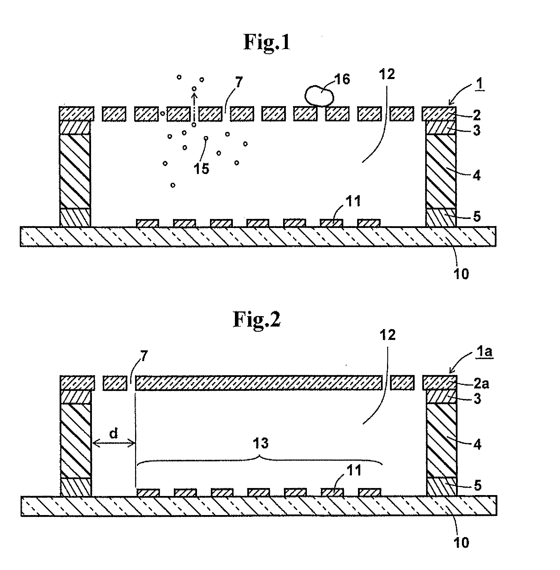
Provided are a pellicle for lithography which can prevent a haze from being generated on a photomask even if a short wave length laser such as an ArF excimer laser is used for a long period of time, and a method for producing a pellicle film to be attached to the pellicle for lithography. The pellicle 1 for lithography is comprised of a frame-like pellicle frame 4 having one open frame on one side of the pellicle frame and another open frame on another side of the pellicle frame; and a laser beam transmissive pellicle film 2 for lithography, which is attached to the one side of the pellicle frame. The another open frame is capable of attaching to a photomask 10 and the pellicle film has a venting hole 7 having a hole size through which a gas molecule 15 can pass but not a foreign particle 16.

Description

TECHNICAL FIELDThe present invention relates to a pellicle for lithography, which is attached to a photomask for lithography used in manufacturing a semiconductor integrated circuit or a liquid crystal display panel etc. to prevent foreign materials from adhering to the photomask, and to a method for manufacturing a pellicle film.BACKGROUND OF THE INVENTIONA minute circuit pattern of the semiconductor integrated circuit or the liquid crystal display panel is formed using lithographic technology in which the circuit pattern is irradiated with a laser beam through a photomask and transferred onto a semiconductor wafer or liquid crystal original plate.Formation of the circuit pattern using this lithographic technology is usually carried out in a clean room, but even in the clean room there are minute foreign particles such as dust. If the foreign particle adheres to the photomask, the particle causes reflection, shading and scattering of light, and therefore deformation and disconnecti...

Claims


Application Information

Patent Timeline
IPC IPC(8): G03F1/00B65D85/86G03F1/62
CPCG03F1/62G03F1/66H01L21/0274H01L21/0337
Inventor SHIRASAKI, TORUITO, KUNIHIRO
Owner SHIN ETSU CHEM IND CO LTD
Why Eureka
Try Eureka