Display device for controlling an organic light emitting layer thickness

a technology of display device, which is applied in the direction of discharge tube luminescnet screen, discharge tube/lamp details, electric discharge lamps, etc., can solve the problems of difficult to maintain the organic light emitting layer at a uniform film thickness, and achieve the effect of achieving uniform illumination

Active Publication Date: 2013-10-01
JOLED INC
View PDF61 Cites 13 Cited by
  • Summary
  • Abstract
  • Description
  • Claims
  • Application Information

AI Technical Summary

Benefits of technology

[0017]The film thickness of the organic light emitting layer after drying tends to establish an inverse relationship with the relative size of the inclination angle of the side wall of the bank. Therefore, the film thickness at the location corresponding to the first side wall tends to become thinner than at the location corresponding to the second side wall. Accordingly, in a display device according to an aspect of the present invention, even if a vapor stream is produced during drying, making the film thickness at the first side wall tend to become thicker, the reduction in film thickness due to making the inclination angle of the first side wall larger offsets this tendency. Therefore, it is possible to make the film shape of the organic light emitting layer in the peripheral light emitting cell uniform.

Problems solved by technology

It is considered difficult, however, to use the technology suggested in Patent Literature 1 over the entire panel of a display device (central region, peripheral region) to form a minute convexity on the inner surface of the bank to a high degree of precision in accordance with each panel region.
Therefore, it is not easy to maintain the organic light emitting layer at a uniform film thickness over the entire panel of a display device (central region, peripheral region).

Method used


Image

  • Display device for controlling an organic light emitting layer thickness
  • Display device for controlling an organic light emitting layer thickness
  • Display device for controlling an organic light emitting layer thickness

Examples


embodiment

[0067]The following describes an example of an embodiment of the present invention with reference to the drawings.

[0068]Note that the following Embodiment is simply an example to clearly illustrate a structure of the present invention and the effects and advantages thereof. The present invention is in no way limited to the following Embodiment except in its essential characteristic elements.

(Process by which the Embodiment According to the Present Invention was Achieved)

[0069]As a result of intense study, the inventor of the present invention discovered the following with regard to the organic light emitting display device recited in the Background Art.

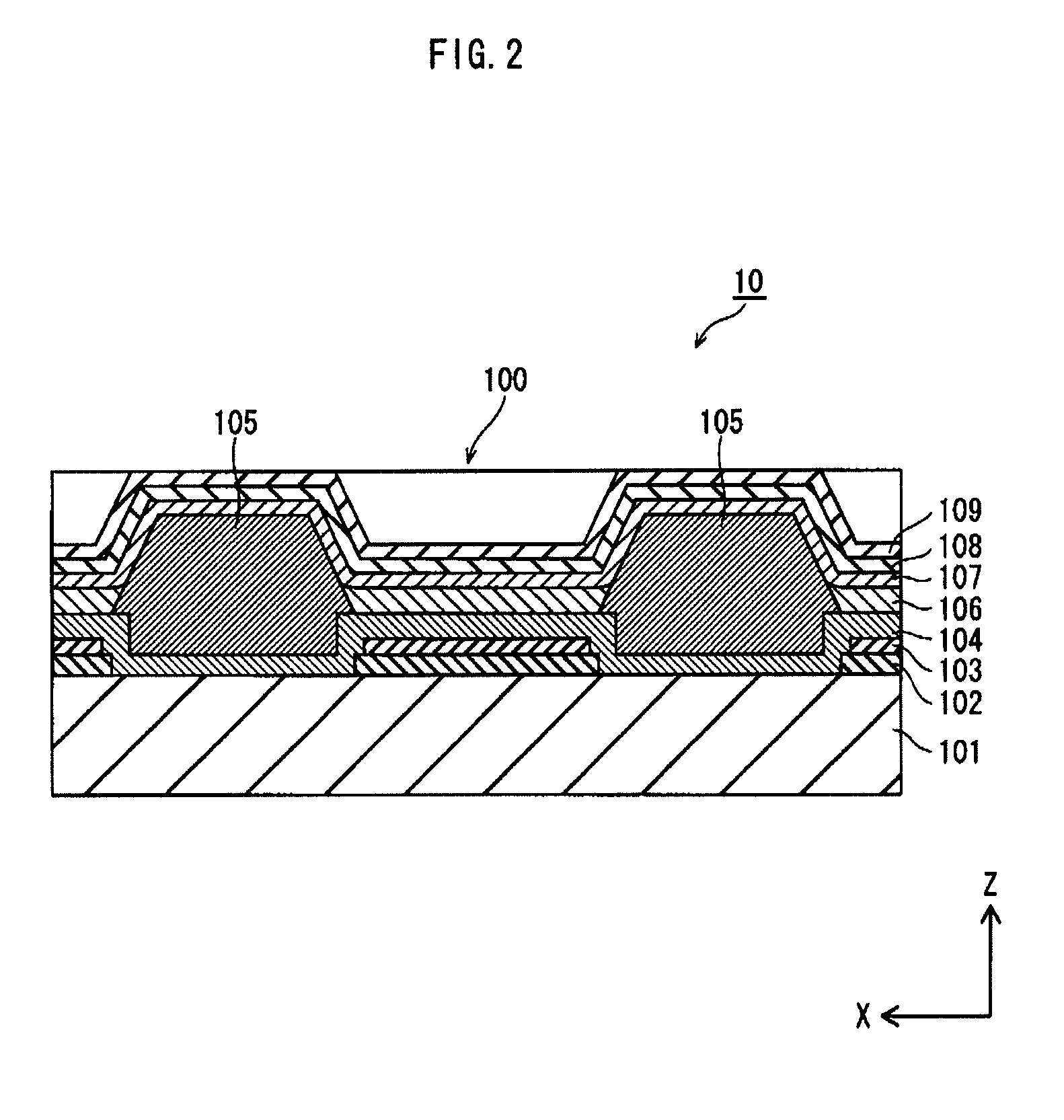
[0070]Normally, as shown in FIG. 17A, an organic light emitting layer 906a, 906c is formed between banks 905 provided above a substrate 901.

[0071]The inventor determined that in this case, as shown in FIG. 17B, the organic light emitting layer 906c at the light emitting cell at the peripheral region of the panel tends to have a less u...

modification 1

[Modification 1]

[0133]Next, with reference to FIG. 11, Modification 1 of the manufacturing method of the display device 1 is described. FIG. 11 shows processes corresponding to the processes shown from FIG. 9C to FIG. 10A.

[0134]As shown in FIG. 11, after layering a bank material layer 1050 on top of the hole injection transporting layer 104, a mask 503 is placed above the bank material layer 1050. The mask 503 has optical transmission sections 503a, 503c1, 503c2, . . . . The optical transmission sections 503a, 503c1, 503c2, . . . are provided in correspondence to the locations where the banks 105a-105f, . . . are to be formed.

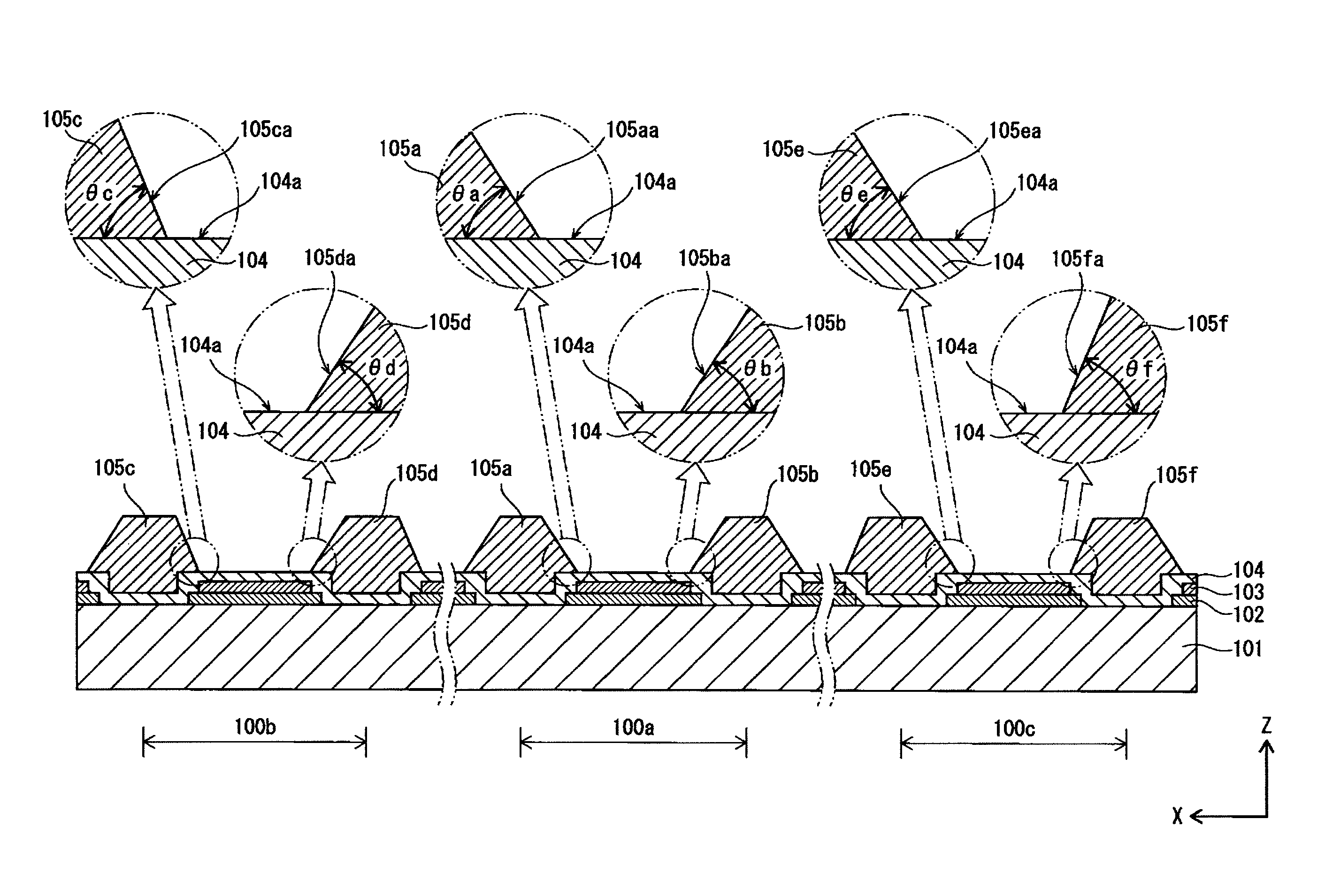
[0135]In the manufacturing method of the display device 1 according to Modification 1, the width Wa of the optical transmission sections 503a, in the region corresponding to the light emitting cell 100a, is defined by the points Pa1 and Pa2 at the bottom edges of the banks 105a and 105b (see FIG. 4) that are being formed.

[0136]On the other hand, the width Wc2 o...

modification 2

[Modification 2]

[0142]Next, with reference to FIGS. 12 and 13, Modification 2 of the manufacturing method of the display device 1 is described. FIGS. 12 and 13 show processes corresponding to the processes shown from FIG. 9C to FIG. 10B.

[0143]As shown in FIG. 12A, after layering a bank material layer 1050 on top of the hole injection transporting layer 104, a mask 504 is placed above the bank material layer 1050. The mask 504 has openings 504a, 504c, . . . corresponding to the sections at which banks 105 are to be formed.

[0144]The openings 504a, provided at locations where the banks 105a and 105b (see FIG. 4) are to be formed in correspondence with the light emitting cell 100a, are formed to have the same width as the openings 501a in the mask 501 used in the manufacturing method of the above Embodiment. On the other hand, a width Wc3 of the openings 504c, provided at locations where the banks 105e and 105f (see FIG. 4) are to be formed in correspondence with the light emitting cell...


PUM


Abstract

A display device includes an array of light emitting cells. Each of the light emitting cells includes a first electrode, a second electrode, and an organic light emitting layer located between the first electrode and the second electrode. Banks are above the first electrode that partition the organic light emitting layer to define each of the light emitting cells. The light emitting cells include a peripheral light emitting cell that is located in a peripheral region of the array. The banks include first and second banks that each border the peripheral light emitting cell. The first bank is closer to a periphery of the array than the second bank. An inclination angle of an innermost sidewall of the first bank that is adjacent the peripheral light emitting cell is greater than an inclination angle of an outermost sidewall of the second bank that is adjacent the peripheral light emitting cell.

Description

CROSS REFERENCE TO RELATED APPLICATION[0001]This is a continuation application of PCT Application No. PCT / JP09 / 007118 filed Dec. 22, 2009, designating the United States of America, the disclosure of which, including the specification, drawings and claims, is incorporated herein by reference in its entirety.BACKGROUND OF THE INVENTION[0002]1. Field of the Invention[0003]The present invention relates to a display device and a manufacturing method thereof, and in particular to a display device provided with an organic light emitting layer and a manufacturing method thereof.[0004]2. Description of the Related Art[0005]In recent years, progress has been made in the research and development of display devices that use the phenomenon of electroluminescence occurring in organic material. Each light emitting cell of such a display device is composed of an anode and a cathode with an organic light emitting layer therebetween. When the display device is driven, light is produced when holes and...

Claims


Application Information

Patent Timeline
Patent Type & Authority Patents(United States)
IPC IPC(8): H01L29/18H01J1/62H01J63/04H01L33/00
CPCH01L27/3246H10K59/122H01L21/0274H10K71/00
Inventor MATSUSHIMA, HIDEAKI
Owner JOLED INC
Why Eureka
Try Eureka