Thin film transistor and method of manufacturing the same

Inactive Publication Date: 2013-07-11
SAMSUNG DISPLAY CO LTD
View PDF12 Cites 10 Cited by
  • Summary
  • Abstract
  • Description
  • Claims
  • Application Information

AI Technical Summary

Benefits of technology

The present invention provides a thin film transistor (TFT) with a thicker conductive pattern to decrease resistance and area. The TFT use a soluble semiconductor material to simplify the manufacturing process and reduce manufacturing costs. The thickness of the gate, source, and drain electrodes leads to increased resistance and area of the TFT, but the use of an organic layer with a trench and soluble semiconductor material simplifies the manufacturing process and reduces manufacturing costs.

Problems solved by technology

In addition, the gate conductive pattern, the data conductive pattern and the semiconductor layer may be manufactured using vacuum conditions so that a manufacturing process may be relatively complicated and manufacturing costs may thereby increase.

Method used


Image

  • Thin film transistor and method of manufacturing the same
  • Thin film transistor and method of manufacturing the same
  • Thin film transistor and method of manufacturing the same

Examples


Embodiment Construction

[0047]Hereinafter, exemplary embodiments of the present invention will be described in further detail with reference to the accompanying drawings.

[0048]In the drawings, the thickness of layers, films, panels, regions, etc., may be exaggerated for clarity. It will be understood that when an element such as, for example, a layer, film, region, or substrate is referred to as being “on”, “connected to” or “coupled to” another element, it can be directly on, connected to or coupled to the other element or intervening elements may also be present. Like reference numerals designate like elements throughout the specification.

[0049]As used herein, the singular forms, “a”, “an”, and “the” are intended to include plural forms as well, unless the context clearly indicates otherwise.

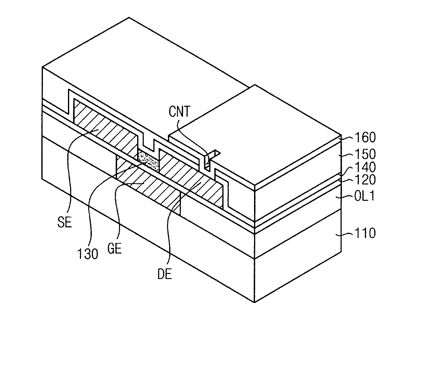
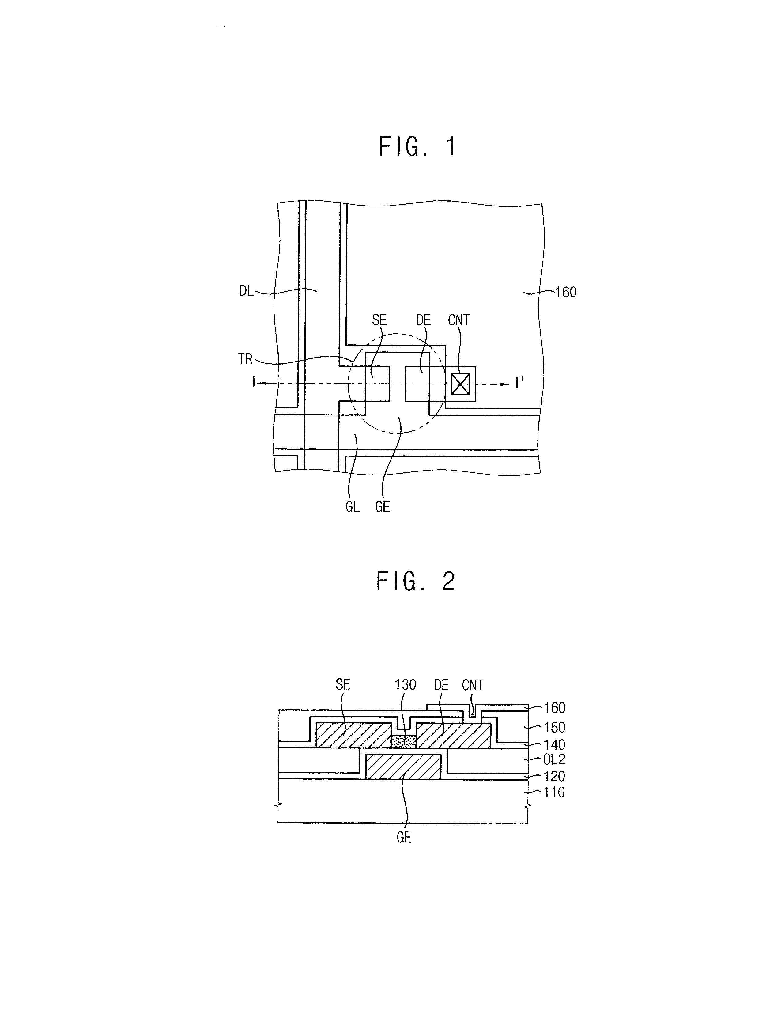
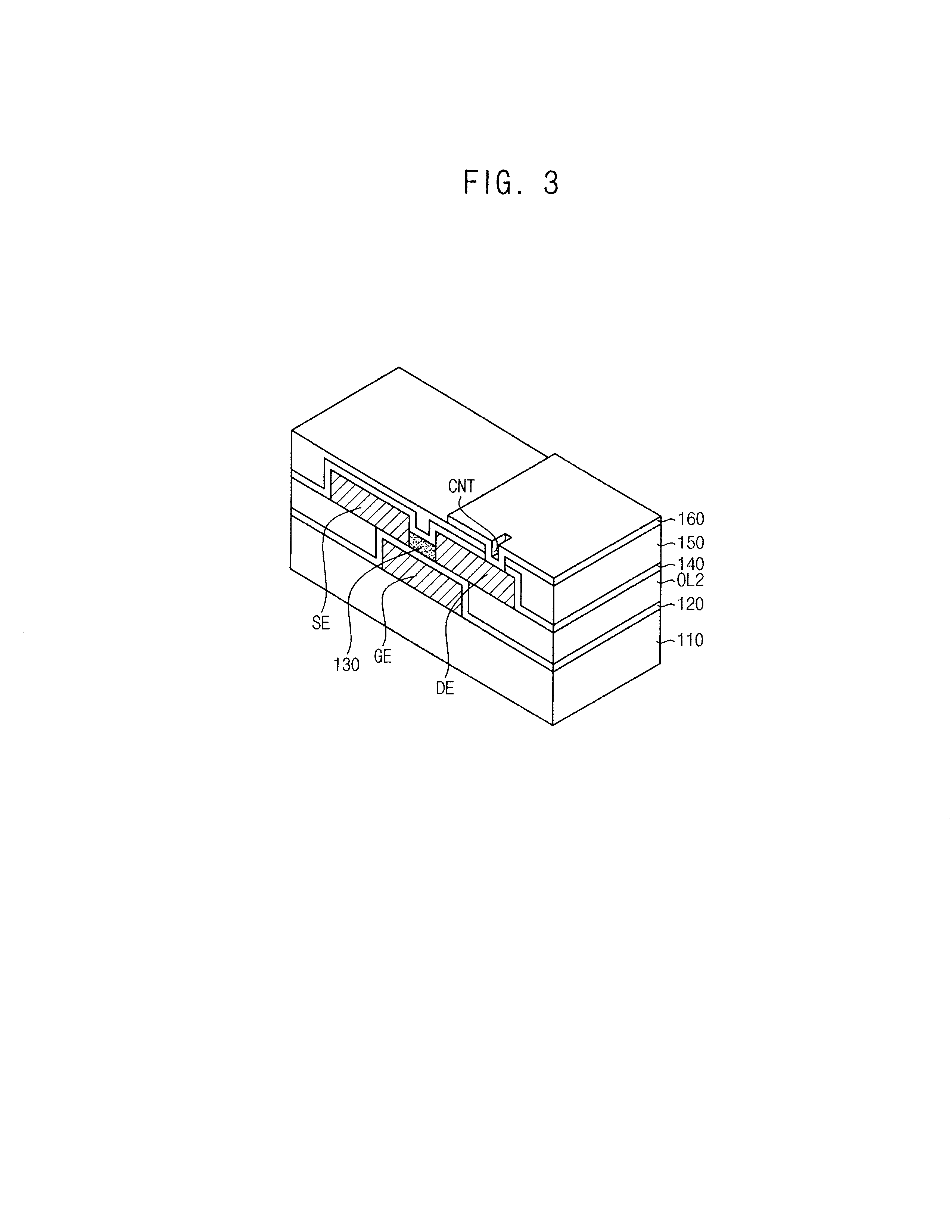
[0050]FIG. 1 is a plan view illustrating an array substrate according to an exemplary embodiment of the present invention.

[0051]Referring to FIG. 1, the array substrate includes, for example, a gate line GL formed on...


PUM


Abstract

A thin film transistor (“TFT”) includes a gate electrode, a gate insulating layer, a source electrode, a drain electrode and a semiconductor layer. The gate insulating layer is disposed on the gate electrode. The source electrode is disposed on the gate insulating layer. The drain electrode is disposed on the gate insulating layer. The drain electrode is spaced apart from the source electrode. The semiconductor layer is disposed on the gate insulating layer. The semiconductor layer makes contact with a side surface of the source electrode and a side surface of the drain electrode.

Description

CROSS-REFERENCE TO RELATED APPLICATION[0001]This application claims priority to Korean Patent Application No. 2012-0002996, filed on Jan. 10, 2012, the disclosure of which is hereby incorporated by reference herein in its entirety.[0002]1. Technical Field[0003]Exemplary embodiments of the present invention relate to a thin film transistor and a method of manufacturing the thin film transistor. More particularly, exemplary embodiments of the present invention relate to a thin film transistor decreasing a resistance and an area and simplifying a manufacturing process and a method of manufacturing the thin film transistor.[0004]2. Discussion of the Related Art[0005]A display apparatus may include, for example, an array substrate including a switching element and an opposite substrate facing the array substrate. The switching element may include a gate electrode electrically connected to a gate line, a semiconductor layer insulated from the gate electrode, a source electrode electricall...

Claims


Application Information

Patent Timeline
IPC IPC(8): H01L29/78H01L21/441
CPCH01L51/0541H10K10/464H01L29/78696H01L29/7869H01L29/0669H01L29/1606H01L29/4908H01L29/45
Inventor SUNG, WOO-YONGKIM, DONG-HWANLEE, JEONG-HOCHA, TAE-WOONCHOI, SANG-GUN
Owner SAMSUNG DISPLAY CO LTD
Why Eureka
Try Eureka