Organic light emitting display

a technology of organic light and display, applied in the direction of instruments, static indicating devices, etc., can solve the problems of increasing the emission period of luminance recovery data, reducing the luminance non-uniformity of external compensation methods, etc., and achieve the effect of minimizing the luminance deviation

Active Publication Date: 2016-11-15
LG DISPLAY CO LTD
View PDF3 Cites 2 Cited by
  • Summary
  • Abstract
  • Description
  • Claims
  • Application Information

AI Technical Summary

Benefits of technology

[0014]Embodiments of the invention provide an organic light emitting display capable of minimizing a luminance deviation between a display line, on which real-time sensing is performed, and a display line, on which the real-time sensing is not performed, when changes in electrical characteristic of a driving thin film transistor (TFT) are compensated in real time using an external compensation method.

Problems solved by technology

The external compensation method reduces the luminance non-uniformity resulting from changes in the electrical characteristic of the driving TFT.
However, as the display line, on which the RT sensing is performed, approaches the lower part of the display panel, the length of the emission period of the luminance recovery data increases.

Method used


Image

  • Organic light emitting display
  • Organic light emitting display
  • Organic light emitting display

Examples


Embodiment Construction

[0042]Reference will now be made in detail to embodiments of the invention, examples of which are illustrated in the accompanying drawings. Wherever possible, the same reference numbers will be used throughout the drawings to refer to the same or like parts. It will be paid attention that detailed description of known arts will be omitted if it is determined that the arts can mislead the embodiments of the invention.

[0043]Exemplary embodiments of the invention will be described with reference to FIGS. 3 to 13.

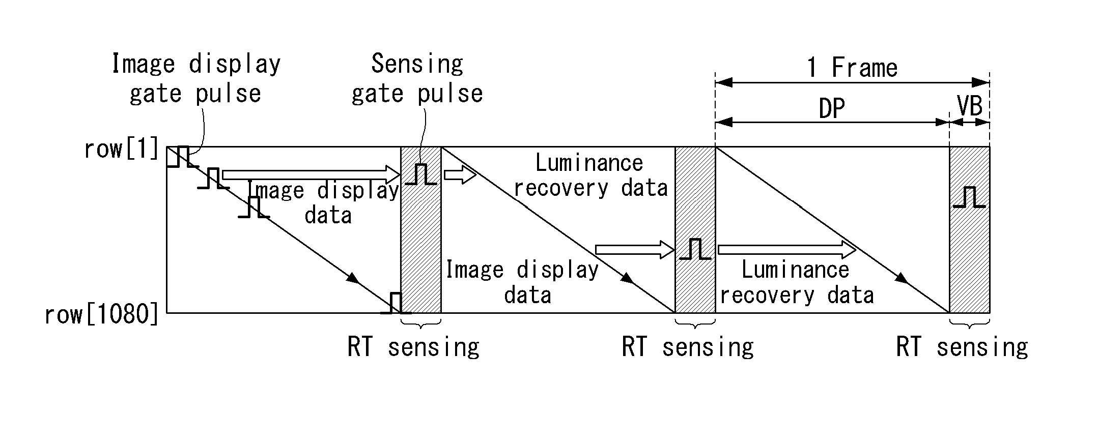
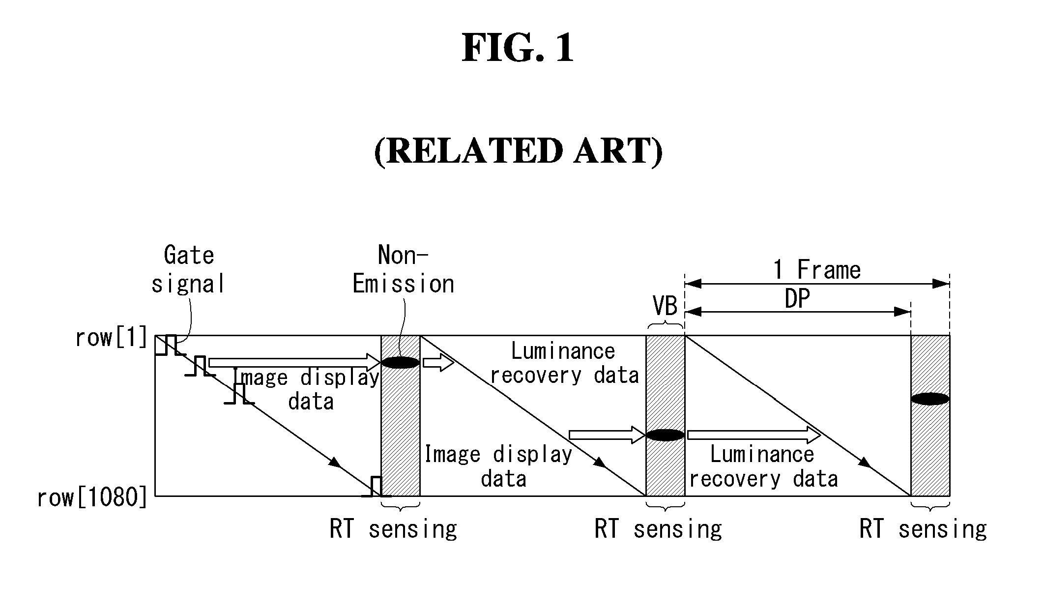
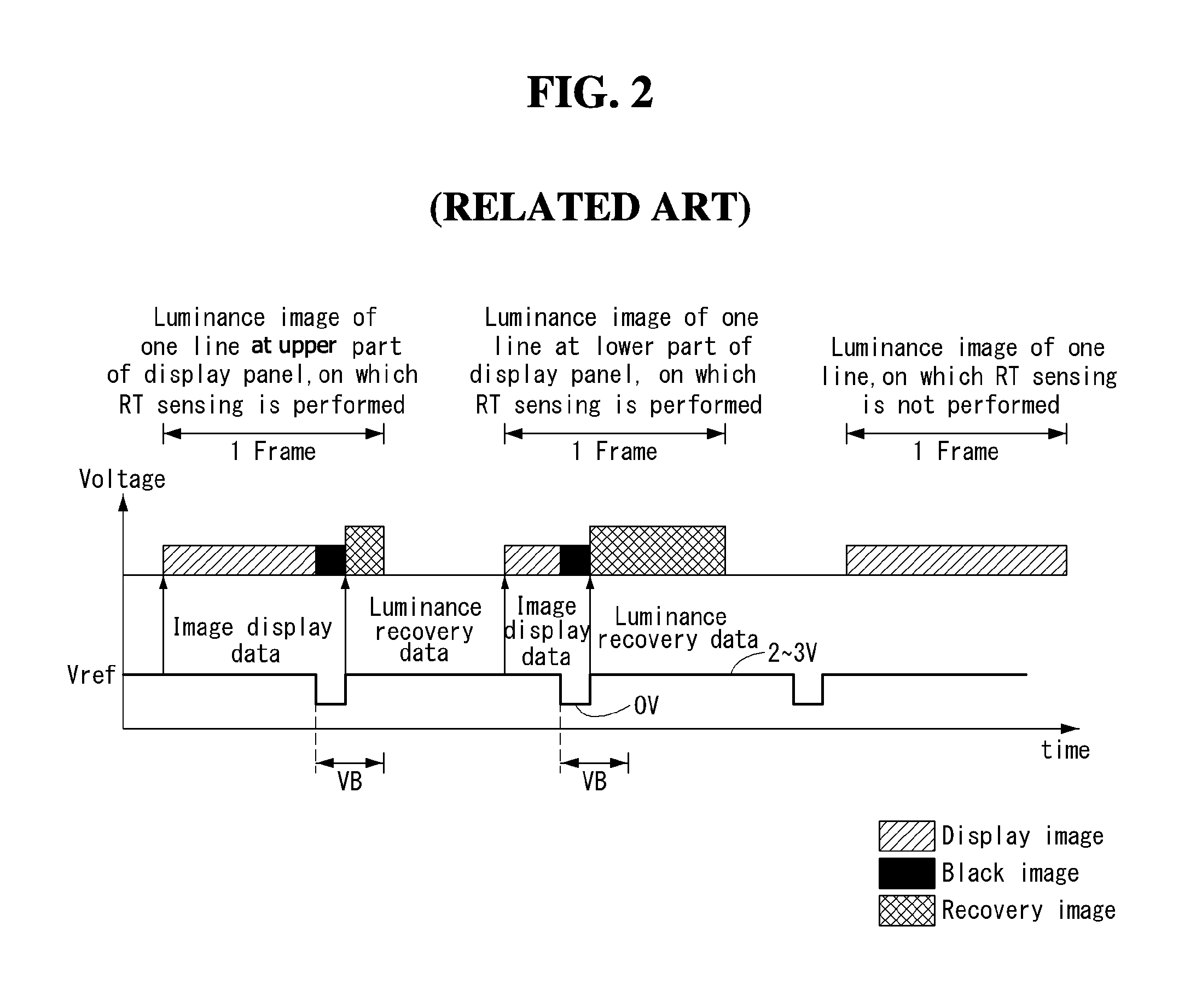
[0044]FIG. 3 is a block diagram of an organic light emitting display according to an exemplary embodiment of the invention. FIG. 4 shows a pixel array of a display panel shown in FIG. 3. FIG. 5 illustrates an RT (real-time) compensation technology according to the embodiment of the invention, in which RT sensing is performed in a vertical blank period.

[0045]As shown in FIGS. 3 and 4, the organic light emitting display according to the embodiment of the invention includes a disp...


PUM


Abstract

An organic light emitting display includes a display panel including display lines, on which a plurality of pixels each including an organic light emitting diode and a driving thin film transistor (TFT) are formed. The display lines are sequentially charged to an image display data voltage in response to an image display gate pulse in an image display period of one frame. A sensing target display line among the display lines outputs a sensing voltage corresponding to changes in electrical characteristic of the driving TFT included in each pixel in response to a sensing gate pulse during a vertical blank period excluding the image display period from the one frame and then is charged to a luminance recovery data voltage. The sensing gate pulse is supplied in the same pulse shape as the image display gate pulse in a predetermined period for charging the luminance recovery data voltage.

Description

[0001]This application claims the benefit of Korea Patent Application No. 10-2013-0166678 filed on Dec. 30, 2013, which is incorporated herein by reference for all purposes as if fully set forth herein.BACKGROUND OF THE INVENTION[0002]1. Field of the Invention[0003]Embodiments of the invention relate to an active matrix organic light emitting display.[0004]2. Discussion of the Related Art[0005]An active matrix organic light emitting display includes organic light emitting diodes (“OLEDs”) capable of emitting light by itself and has advantages of a fast response time, a high light emitting efficiency, a high luminance, a wide viewing angle, and the like.[0006]The OLED serving as a self-emitting element includes an anode electrode, a cathode electrode, and an organic compound layer formed between the anode electrode and the cathode electrode. The organic compound layer includes a hole injection layer HIL, a hole transport layer HTL, a light emitting layer EML, an electron transport la...

Claims


Application Information

Patent Timeline
Patent Type & Authority Patents(United States)
IPC IPC(8): G09G3/30G09G3/32
CPCG09G3/3233G09G3/3291G09G2310/0254G09G2320/0233G09G2320/0295G09G2320/043G09G2320/045G09G3/32
Inventor TANI, RYOSUKEHONG, SUNGJINNAM, WOOJINPARK, JOONMINLEE, SEONMIYANG, INYOUNGLEE, JONGHO
Owner LG DISPLAY CO LTD
Why Eureka
Try Eureka