
Liquid crystal display device and method for manufacturing the same
Patent Information
- Authority / Receiving Office
- US · United States
- Current Assignee / Owner
- Publication Date
- 2007-03-29
- Estimated Expiration
- Not applicable · inactive patent
Smart Images
Figure 1 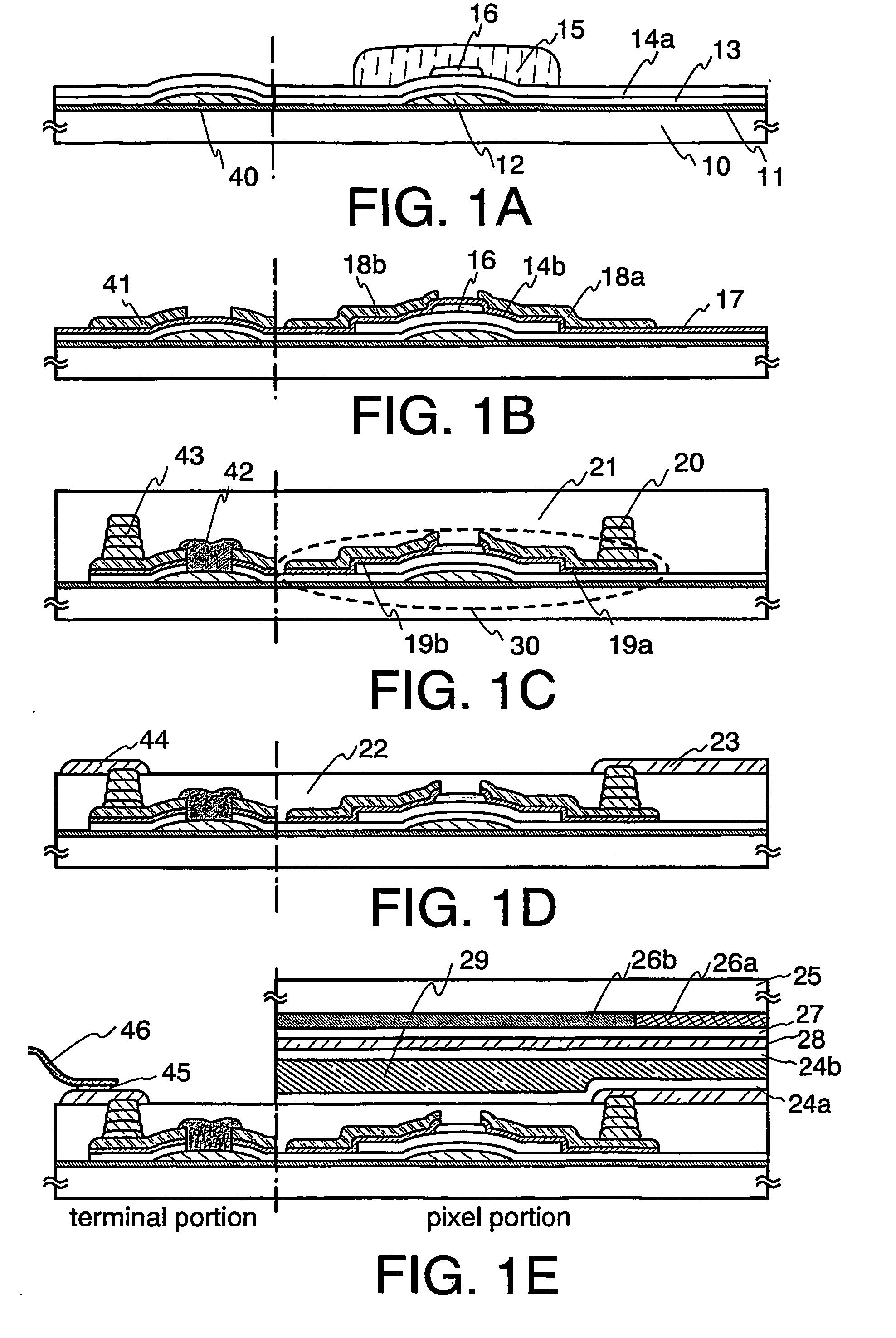
Figure 2 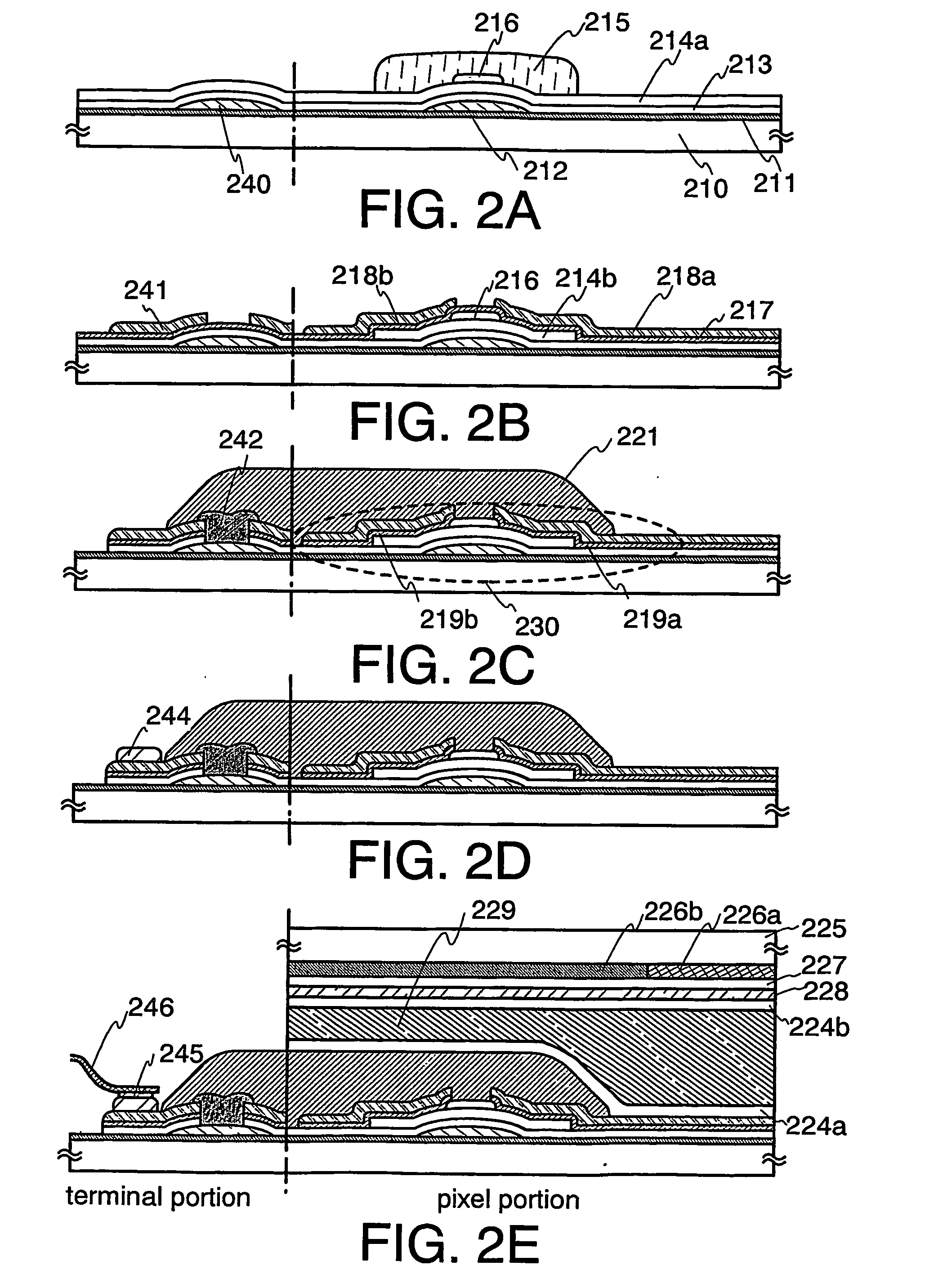
Figure 3
Abstract
Description
TECHNICAL FIELD
[0001] The present invention relates to a semiconductor device having a circuit that is composed of a thin film transistor (hereinafter referred to as TFT) and a method for manufacturing the semiconductor device. An example of the semiconductor device is electronic device having an electro-optical device typified by a liquid crystal display device as one of its parts.
[0002] In this specification, the term semiconductor device refers to devices that function by utilizing semiconductor characteristics. Further, electro-optical devices, semiconductor circuits, and electronic devices are all regarded as semiconductor devices. BACKGROUND ART
[0003] In late years, a technology for forming a thin film transistor (TFT) using a semiconductor thin film (a thickness of around several nanometers to several hundred nanometers) formed over a substrate having an insulating surface has been attracting attention. Thin film transistors are broadly applied to electronic devices such a...
Examples
embodiment mode 1
[0048] Here, a method for manufacturing an active matrix liquid crystal display device using an inverted staggered TFT as a switching element will be described. FIG. 1 shows a cross section of the manufacturing process.
[0049] First, a base film 11 for improving adhesion with a material layer to be later formed by a droplet discharge method is formed over a substrate 10. The base film 11 may be formed thin; accordingly, it can be regarded as base pretreatment. A photocatalyst (titanium oxide (TiO2), strontium titanate (SrTiO3), cadmium selenide (CdSe), potassium tantalate (KTaO3), cadmium sulfide (CdS), zirconium oxide (ZrO2), niobium oxide (Nb2O5), zinc oxide (ZnO), iron oxide (Fe2O3), tungsten oxide (WO3)) may be applied with a spray; alternatively, an organic material (polyimide, acryl, or a material having a skeletal structure including a bond of silicon (Si) and oxygen (O) which contains at least one of the group consisting of hydrogen, fluorine, alkyl group and aromatic hydroc...
embodiment mode 2
[0093] Here, an example in which the connection method is different from Embodiment Mode 1 will be shown. FIG. 2A to 2E show a cross section of manufacturing steps of an active matrix liquid crystal display device using an inverted staggered TFT as a switching element.
[0094] First, a state equivalent to FIG. 1A is made according to the steps shown in Embodiment Mode 1. A base film 211, a metal wiring 212, a wiring 240 extending to a terminal area are formed over a substrate 210. Further, a gate insulating film 213, a semiconductor film 214a, and an insulating layer 216 are sequentially formed thereover. A mask 215 covering the insulating layer 216 is formed by a droplet discharge method (FIG. 2A).
[0095] Next, a semiconductor film 214a except the area covered with the mask 215 is removed by dry etching or wet etching, so that a semiconductor layer 214b to be an active layer is formed.
[0096] After the mask 215 is removed, an n-type semiconductor film 217 is formed over the entire s...
embodiment mode 3
[0114] Here, an example in which the connection method is different from Embodiment Mode 1 will be shown. FIGS. 3A to 3D show a cross section of manufacturing steps of an active matrix liquid crystal display device using an inverted staggered TFT as a switching element.
[0115] First, a state equivalent to FIG. 1C is made according to the steps shown in Embodiment Mode 1. A base film 311, a metal wiring 312, a wiring 340 extending to a terminal area are formed over a substrate 310. Further, a gate insulating film 313, a semiconductor film, and an insulating layer 316 are sequentially formed thereover. A mask covering the insulating layer 316 is formed by a droplet discharge method. Next, a semiconductor film except the area covered with the mask is removed by dry etching or wet etching, so that a semiconductor layer 314 to be an active layer is formed. After the mask is removed, an n-type semiconductor film is formed over the entire surface. Next, a composition-containing a conductiv...