Charge pump circuit

A charge pump and circuit technology, applied in the direction of conversion equipment without intermediate conversion to AC, can solve the problems of obvious streak image quality, deterioration, increase charge pump circuit, etc., to reduce voltage surge noise, The effect of stable output voltage and slowing down the instantaneous voltage change

Inactive Publication Date: 2008-10-01
NOVATEK MICROELECTRONICS CORP
View PDF0 Cites 7 Cited by
  • Summary
  • Abstract
  • Description
  • Claims
  • Application Information

AI Technical Summary

Problems solved by technology

In the application of the display panel, the reduced charge pumping circuit usually increases the operating frequency of the charge pumping circuit because of insufficient driving capability. The shortcoming is that more and continuous voltage surges will be generated, and in severe cases, the picture will appear obviously. streaks and degrades the picture quality

Method used


Image

  • Charge pump circuit
  • Charge pump circuit
  • Charge pump circuit

Examples


Embodiment Construction

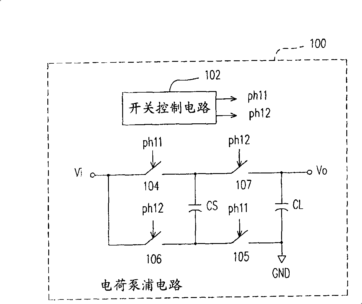
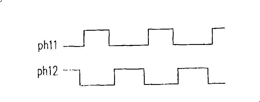
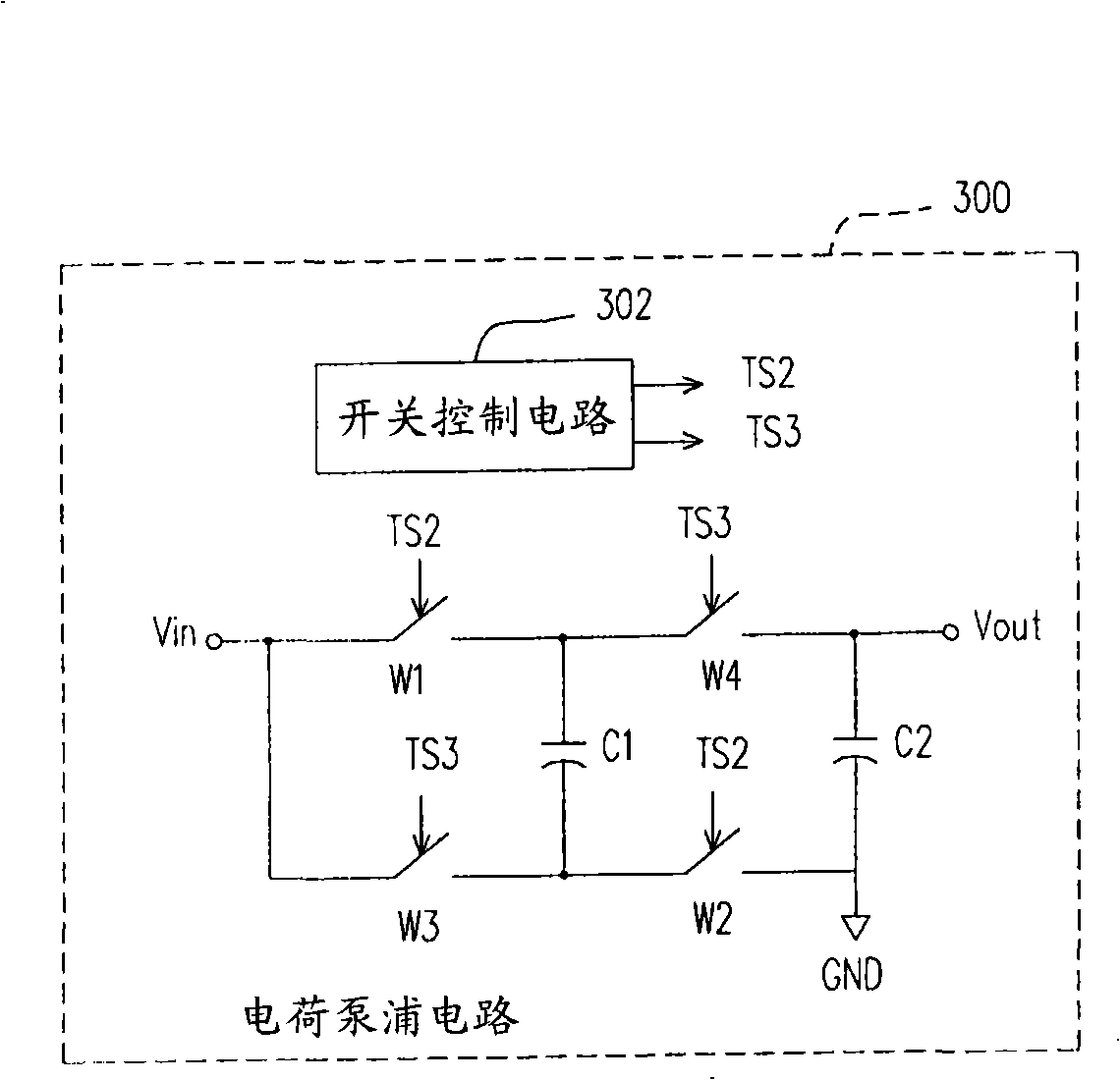
[0045] Please refer to image 3 , image 3It is a circuit diagram of a charge pump according to an embodiment of the present invention. The charge pumping circuit 300 is suitable for a display panel. The charge pumping circuit 300 includes a switch control circuit 302, switches W1-W4, a capacitor C1, and a capacitor C2, wherein each switch (W1-W4) has a first terminal, The second terminal and the control terminal, each capacitor has a first terminal and a second terminal. The coupling relationship of the above-mentioned components is as follows. A first terminal of the switch W1 is coupled to an input voltage Vin, and a second terminal of the switch W1 is coupled to a first terminal of the switch W4 and a first terminal of the capacitor C1. A first terminal of the switch W3 is coupled to the input voltage Vin and the first terminal of the switch W1 , and a second terminal of the switch W3 is coupled to the first terminal of the switch W2 and the second terminal of the capac...


PUM


Abstract

The present invention provides a charge pump circuit which is suitable to be used in a display panel. The charge pump circuit comprises a plurality of switches and a switch controlling circuit. First of all, the transition states of a plurality of switches are defined: the state switching from non-conducting state to conducting state is called an enabling transition, and the state switching from conducting state to non-conducting state is called a forbidding transition. The switch controlling circuit is coupled to a plurality of switches and is used for the conducting and non-conducting of a plurality of switches, and further the charge pump circuit is leaded to provide an output voltage different from the input voltage. The switch controlling circuit leads to that the time necessary for the enabling transition of a plurality of switches is longer than the time necessary for the forbidding time, wherein, when a plurality of switches are in the enabling transition, the equivalent impedances of a plurality of switches changes from big to small.

Description

technical field [0001] The invention relates to a charge pumping circuit, in particular to a charge pumping circuit capable of reducing voltage spikes. Background technique [0002] Various levels of voltage sources are often required in electronic devices, and charge pump circuits are usually configured to generate voltage sources of various levels. Many charge pumping circuits are also used in the design of the power supply circuit of the display panel. Please refer to figure 1 , figure 1 It is a known charge pump circuit diagram. The charge pumping circuit 100 includes a switch control circuit 102 , switches 104 - 107 , a capacitor CS, and a capacitor CL. The known switch control circuit 102 generates two non-overlapping frequency signals ph11 and ph12, which are used to control the conduction and non-conduction of the switch 104 to the switch 107. The charge pump circuit 100 thus provides An output voltage Vo different from the input voltage Vi. [0003] figure 2...

Claims


Application Information

Patent Timeline
Patent Type & Authority Applications(China)
IPC IPC(8): H02M3/07
Inventor 颜志仁谢致远
Owner NOVATEK MICROELECTRONICS CORP
Why Eureka
Try Eureka