

Charge pump circuit
A charge pumping and circuit technology, applied in optics, instruments, conversion equipment without intermediate conversion to AC, etc., can solve the problems of obvious streak image quality, deterioration, adding charge pumping circuit, etc., to reduce the voltage The effect of surge noise, stable output voltage, and slowing down the instantaneous voltage change
Inactive Publication Date: 2010-10-13
NOVATEK MICROELECTRONICS CORP
View PDF3 Cites 1 Cited by
- Summary
- Abstract
- Description
- Claims
- Application Information
AI Technical Summary
Problems solved by technology
In the application of the display panel, the reduced charge pumping circuit usually increases the operating frequency of the charge pumping circuit because of insufficient driving capability. The shortcoming is that more and continuous voltage surges will be generated, and in severe cases, the picture will appear obviously. streaks and degrades the picture quality
Method used
View moreImage
Smart ImageViewing Examples

Examples
Embodiment Construction
Login to View More PUM
 Abstract
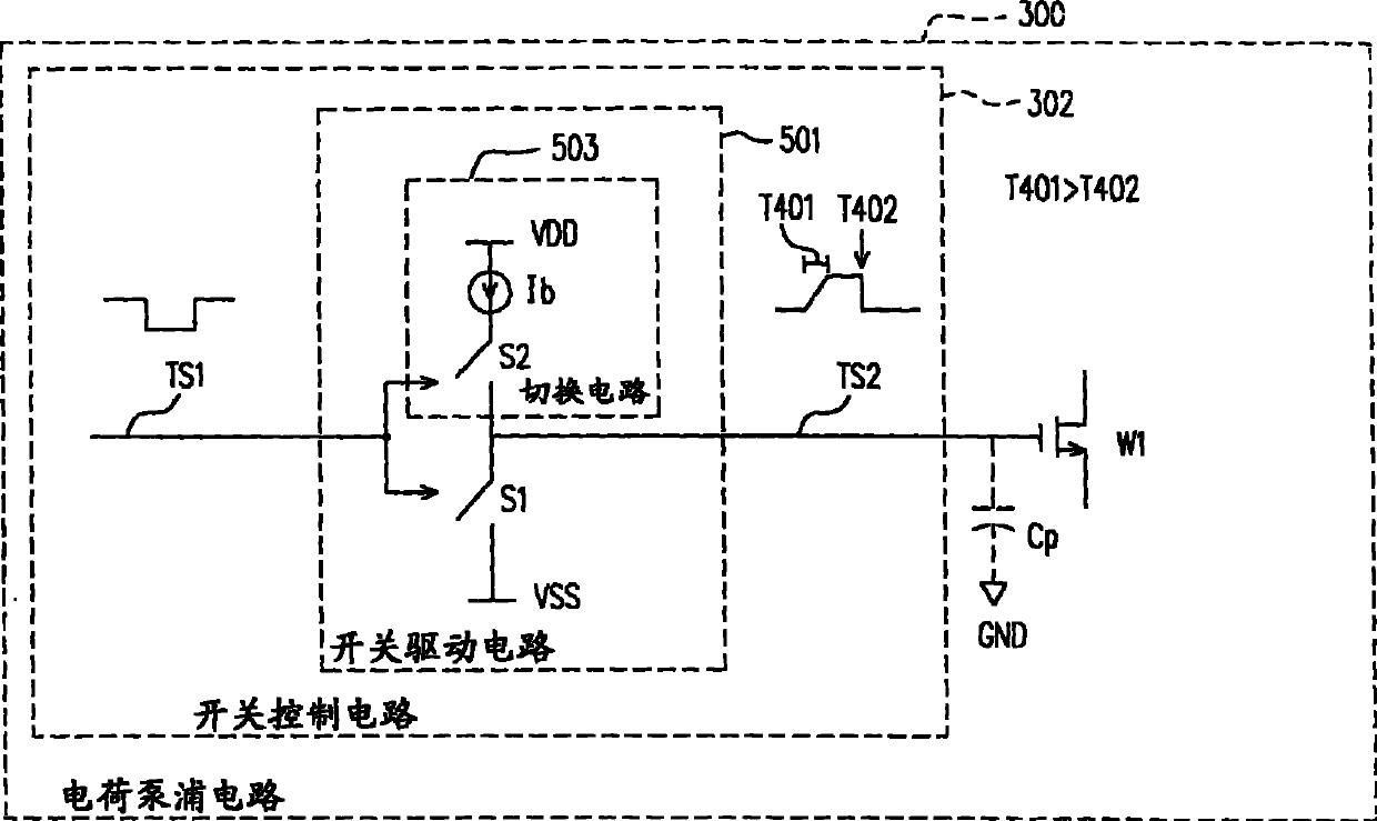
The present invention provides a charge pump circuit which is suitable to be used in a display panel. The charge pump circuit comprises a plurality of switches and a switch controlling circuit. First of all, the transition states of a plurality of switches are defined: the state switching from non-conducting state to conducting state is called an enabling transition, and the state switching from conducting state to non-conducting state is called a forbidding transition. The switch controlling circuit is coupled to a plurality of switches and is used for the conducting and non-conducting of a plurality of switches, and further the charge pump circuit is leaded to provide an output voltage different from the input voltage. The switch controlling circuit leads to that the time necessary for the enabling transition of a plurality of switches is longer than the time necessary for the forbidding time, wherein, when a plurality of switches are in the enabling transition, the equivalent impedances of a plurality of switches changes from big to small.
Description
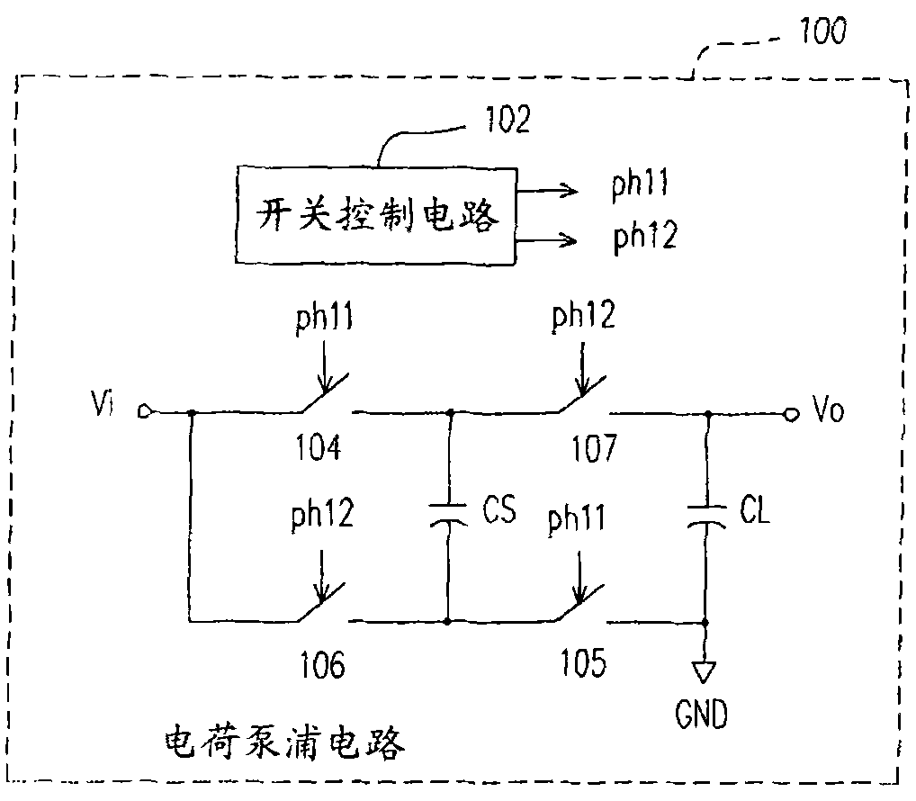
technical field The invention relates to a charge pumping circuit, in particular to a charge pumping circuit capable of reducing voltage surge (vominl. TIFtage spike). Background technique Various levels of voltage sources (vominl. TIFtage source) are often required in electronic devices, and charge pump circuits are usually configured to generate voltage sources of various levels. Many charge pumping circuits are also used in the design of the power supply circuit of the display panel. Please refer to FIG. 1 , which is a known charge pump circuit diagram. The charge pumping circuit 100 includes a switch control circuit 102 , switches 104 - 107 , a capacitor CS, and a capacitor CL. The known switch control circuit 102 generates two frequency signals ph11 and ph12 with non-overminl. Thus an output voltage Vo different from the input voltage Vi is provided. FIG. 2 shows a frequency signal waveform diagram of the switch control circuit 102 in FIG. 1 . When the frequency s...
Claims
Login to View More Application Information
Patent Timeline
 Patent Type & AuthorityPatents(China)
IPC IPC(8): G02F1/00G09G3/00H02M3/07
Inventor颜志仁谢致远
OwnerNOVATEK MICROELECTRONICS CORP