

Semiconductor device and manufacturing method thereof
A manufacturing method and semiconductor technology, which are applied in the fields of semiconductor/solid-state device manufacturing, semiconductor devices, and electric solid-state devices, etc., can solve the problem that the size of the device is difficult to reduce, improve the withstand voltage characteristics, reduce the manufacturing cost, and reduce the number of masks. Effect
- Summary
- Abstract
- Description
- Claims
- Application Information
AI Technical Summary
Problems solved by technology
Method used
Image

Examples
Embodiment Construction
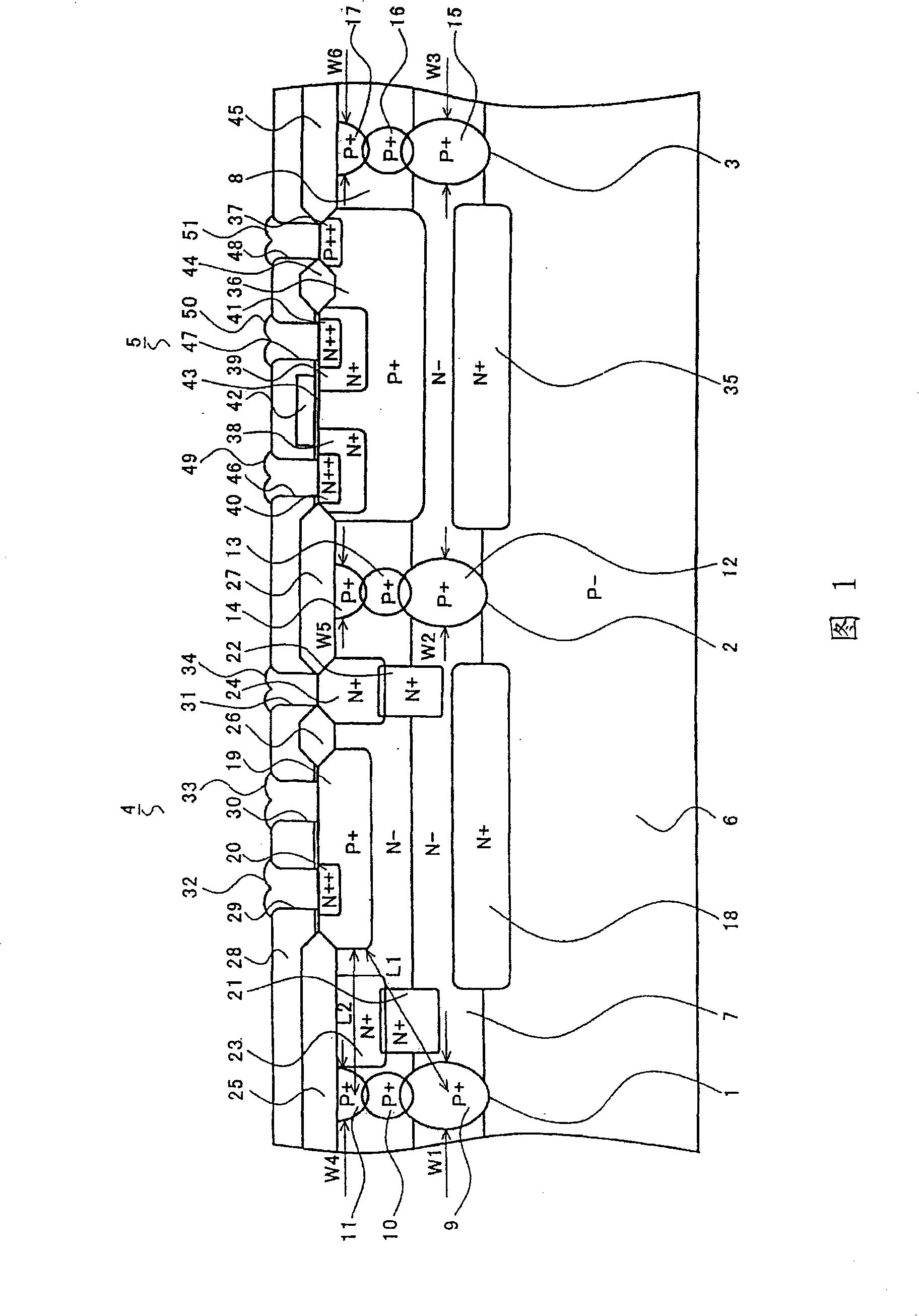
[0061] Refer below figure 1 A semiconductor device according to a first embodiment of the present invention will be described.
[0062] Such as figure 1 As shown, isolation regions (hereinafter referred to as ISOs) 1 to 3 are formed in a grid pattern over the entire IC, and various semiconductor elements are formed in island regions (hereinafter referred to as islands) surrounded by the ISOs. As shown in the figure, an NPN transistor 4 is formed on one island, and an N-channel MOS transistor 5 is formed on the other island.
[0063] First, as shown in the figure, ISOs 1-3 penetrate the first and second N-type epitaxial layers (hereinafter referred to as EPI) 7, 8 on the P-type single crystal silicon substrate 6, and are divided into a plurality of islands. ISO 1 to 3 consist of three snowman-shaped diffusion layers. For example, ISOs 1 to 3 are composed of P-type buried diffusion layers (hereinafter referred to as buried layers) 9 , 10 , 12 , 13 , 15 , and 16 and P-type d...
PUM
 Abstract
Description
Claims
Application Information