
Multilayer ceramic electronic component and manufacturing method thereof

A technology of electronic parts, ceramics, applied in the field of laminated ceramic electronic parts and its manufacture

Active Publication Date: 2012-06-27
MURATA MFG CO LTD
View PDF1 Cites 0 Cited by
  • Summary
  • Abstract
  • Description
  • Claims
  • Application Information

AI Technical Summary

Problems solved by technology

[0008] However, in the case of using the above-mentioned method based on plating, the adhesive effect of glass in the method using conventional conductive paste cannot be obtained. , so there is a problem that the adhesion between the plating film, that is, the external terminal electrode and the ceramic raw material is weak

Method used


Image

  • Multilayer ceramic electronic component and manufacturing method thereof
  • Multilayer ceramic electronic component and manufacturing method thereof
  • Multilayer ceramic electronic component and manufacturing method thereof

Examples


Embodiment Construction

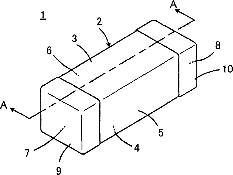
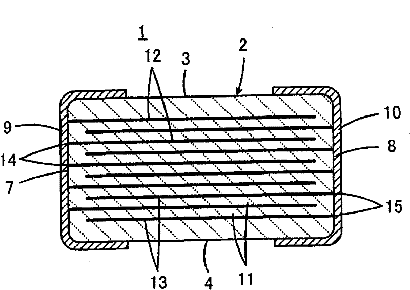
[0060] Figure 1 to Figure 4 It is used to explain the first embodiment of the present invention. here, figure 1 It is a perspective view showing a multilayer ceramic capacitor 1 as an example of a multilayer ceramic electronic component. figure 2 for along figure 1 A profile of the line A-A.

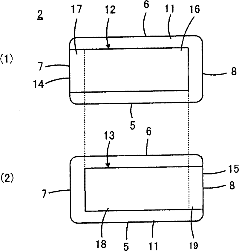
[0061] A multilayer ceramic capacitor 1 includes a ceramic raw material 2 . The ceramic raw material 2 has a cubic shape, and has mutually opposing first and second main surfaces 3 and 4 , and four side surfaces 5 to 8 connecting the first and second main surfaces 3 and 4 . In addition, in the following description, among the four side surfaces 5 to 8, the side surfaces 5 and 6 extending in the longitudinal direction of the main surfaces 3 and 4 are referred to as first and second side surfaces, respectively, and the side surfaces extending in the short direction are referred to as 7 and 8 are referred to as first and second end faces, respectively.

[0062] First and second ex...


PUM

PropertyMeasurementUnit
thicknessaaaaaaaaaa
thicknessaaaaaaaaaa

Abstract

A multilayer ceramic electronic component including thin external terminal electrodes each having a superior bonding force to a ceramic base body is provided. In order to form the external terminal electrodes (9), after Cu plating films (20) are deposited on exposed portions (14) of internal electrodes (12) by direct plating on a ceramic base body (2), a Cu liquid phase, an O2-containing liquid phase, and a Cu solid phase are generated between the Cu plating film (20) and the ceramic base body (2) by a heat treatment, so that Cu oxides (21) are dispersed in the Cu plating film (20), at least near an interface with the ceramic base body (2). Since the Cu oxides (21) function as an adhesive, a bonding force of the Cu plating film (20) to the ceramic base body (2) can be increased, and hencethe external terminal electrode (9) having a superior bonding force to the ceramic base body can be obtained.

Description

technical field [0001] The present invention relates to a laminated ceramic electronic component and a method of manufacturing the same, and more particularly to a structure of an external terminal electrode included in a laminated ceramic electronic component and a method for forming the external terminal electrode. Background technique [0002] In recent years, the market for small mobile electronic devices such as mobile phones, notebook computers, digital cameras, and digital audio equipment has been expanding. In these mobile electronic devices, performance enhancement is advancing along with miniaturization. Many multilayer ceramic electronic components are mounted on mobile electronic devices, but miniaturization and high performance are also required for multilayer ceramic electronic components. For example, multilayer ceramic capacitors are required to be smaller and larger. [0003] As a device for downsizing and increasing the capacity of a multilayer ceramic cap...

Claims


Application Information

Patent Timeline
Patent Type & Authority Patents(China)
IPC IPC(8): H01G4/228H01G4/30H01F17/00
CPCH01G4/232H01G4/30
Inventor 竹内俊介川崎健一元木章博小川诚松本修次西原诚一
Owner MURATA MFG CO LTD
Learn More