Method for constructing fully-digital GNSS compatible navigation receiver

A technology for navigation receivers and construction methods, applied in satellite radio beacon positioning systems, measuring devices, instruments, etc., can solve problems such as difficult implementation, complex functions and structures, and achieve potential interference elimination, good scalability, and reduced The effect of device occupancy

CN101833100BInactive Publication Date: 2012-12-12BEIHANG UNIV
0 Cites 0 Cited by

Patent Information

Authority / Receiving Office
CN · China
Patent Type
Patents(China)
Current Assignee / Owner
Publication Date
2012-12-12
Estimated Expiration
Not applicable · inactive patent

Smart Images

  • Figure 1
    Figure 1
  • Figure 2
    Figure 2
  • Figure 3
    Figure 3
Patent Text Reader

Abstract

The invention relates to a method for constructing a fully-digital GNSS compatible navigation receiver, which comprises four steps: I, constructing a receiving link in accordance with actual needs by taking the characteristics of satellite signals, performance indexes and current device level into comprehensive consideration; II, choosing a proper A / D chip and a proper time clock source to complete direct radio frequency sampling and constructing a sampling rate in accordance with bandwidth sampling requirements; III, constructing a filter decimation network to reduce the sampling rate, completing the down-conversion of the radio frequency, converting the frequency of the bandwidth satellite navigation signals near 1.2G and 1.5G two frequency points down to a low medium frequency under a condition of a high sampling rate, and finally outputting a sampling time clock and a GNSS medium frequency signal; and IV, constructing digital radio frequency front end and rear end medium frequencyreceiver interfaces for making the receiver compatible with other medium frequency receiver. The thought of using software radio realizes the collective receiving of full-range GNSS satellite navigation signals; and the medium frequency receivers can complete navigation solution and output measurement values, so multi-system and multi-frequency point compatible navigation is realized. The method has an application and development prospect in the technical field of communication.
Need to check novelty before this filing date? Find Prior Art

Description

(1) Technical field:

[0001] The invention relates to a construction method of an all-digital GNSS compatible navigation receiver, which is related to the research direction of global satellite navigation system, satellite navigation receiver and software radio, and belongs to the technical field of communication. (two) background technology:

[0002] In recent years, the construction of GNSS satellite navigation system has made great progress, and the demand for low-cost, high-performance, flexible and easy-to-use GNSS compatible receivers has greatly increased in various fields. Generally, navigation receivers adopt an analog multi-stage down-conversion structure, and digitization and signal processing are performed after down-conversion to intermediate frequency. This signal receiving method has poor flexibility and is easy to introduce errors. The GNSS receiver based on the idea of ​​software radio does not need to re-replace equipment for signal structure and system upgr...

Examples

Embodiment Construction

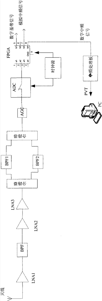
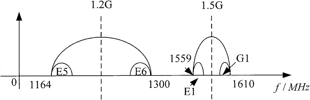
[0031] The overall block diagram of the present invention is as figure 1 shown. The satellite signal is first received by a broadband antenna (3db bandwidth 1.15-1.65GHz), and then amplified by a three-stage low-noise amplifier (LNA). After the first-stage LNA, it passes through a broadband pre-filter with a bandwidth range of about 1.2-1.5GHz. Large broadband; after the last level of LNA, followed by a splitter, divided into two channels, each passing through a bandpass filter, filtering out the navigation frequency band signal with a bandwidth of 136MHz near 1.2G and the navigation signal with a bandwidth of 51MHz near 1.5GHz; filter After being combined by a combiner, the combined frequency band is as follows: figure 2 The signal is then controlled by the AGC and then sampled by the A / D chip with a sampling rate up to 1GHz, and the A / D outputs two signals at half the sampling clock rate; Sampling rate and multi-frequency point signal separation; FPGA output contains data...