Semiconductor grain point measurement machine test method and semiconductor grain point measurement machine

An inspection method and semiconductor technology, which is applied in semiconductor devices, semiconductor/solid-state device testing/measurement, semiconductor/solid-state device manufacturing, etc., can solve problems such as misjudgment of grain detection and plummeting worth, so as to avoid a large number of false detection grains Effect

Inactive Publication Date: 2011-01-26
致茂电子(苏州)有限公司
View PDF0 Cites 16 Cited by
  • Summary
  • Abstract
  • Description
  • Claims
  • Application Information

AI Technical Summary

Problems solved by technology

According to this calibration method, even if there is a serious deviation in the machine between the two calibration actions, there is no appropriate mechanism for warning, and only relying on the vigilance of the operator with experience, even if the machine is stopped for calibration, there are still a large number of misjudged die detection
When the re-inspection misjudged the crystal grains, the surface marks that can be clearly observed by the microscope will be caused when the probe is pressed and poked. This kind of grain is classified as a secondary product and its value plummets

Method used


Image

  • Semiconductor grain point measurement machine test method and semiconductor grain point measurement machine
  • Semiconductor grain point measurement machine test method and semiconductor grain point measurement machine
  • Semiconductor grain point measurement machine test method and semiconductor grain point measurement machine

Examples


Embodiment Construction

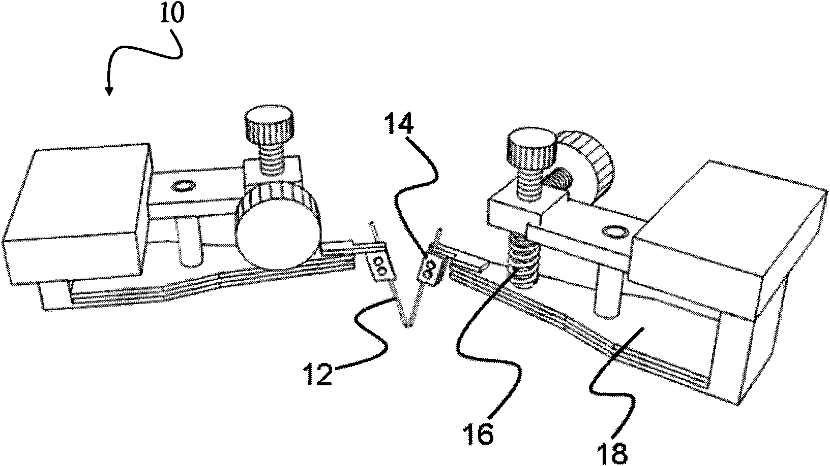
[0033] The aforementioned and other technical contents, features and effects of the present invention will be clearly presented in the following detailed description of preferred embodiments with accompanying drawings. For the convenience of description, the machine inspection method of the present invention is taken as an example of a spot test machine for semiconductor grains for optical inspection, and the control unit and support lines necessary for the base of the machine are omitted to avoid confusion in the drawing.

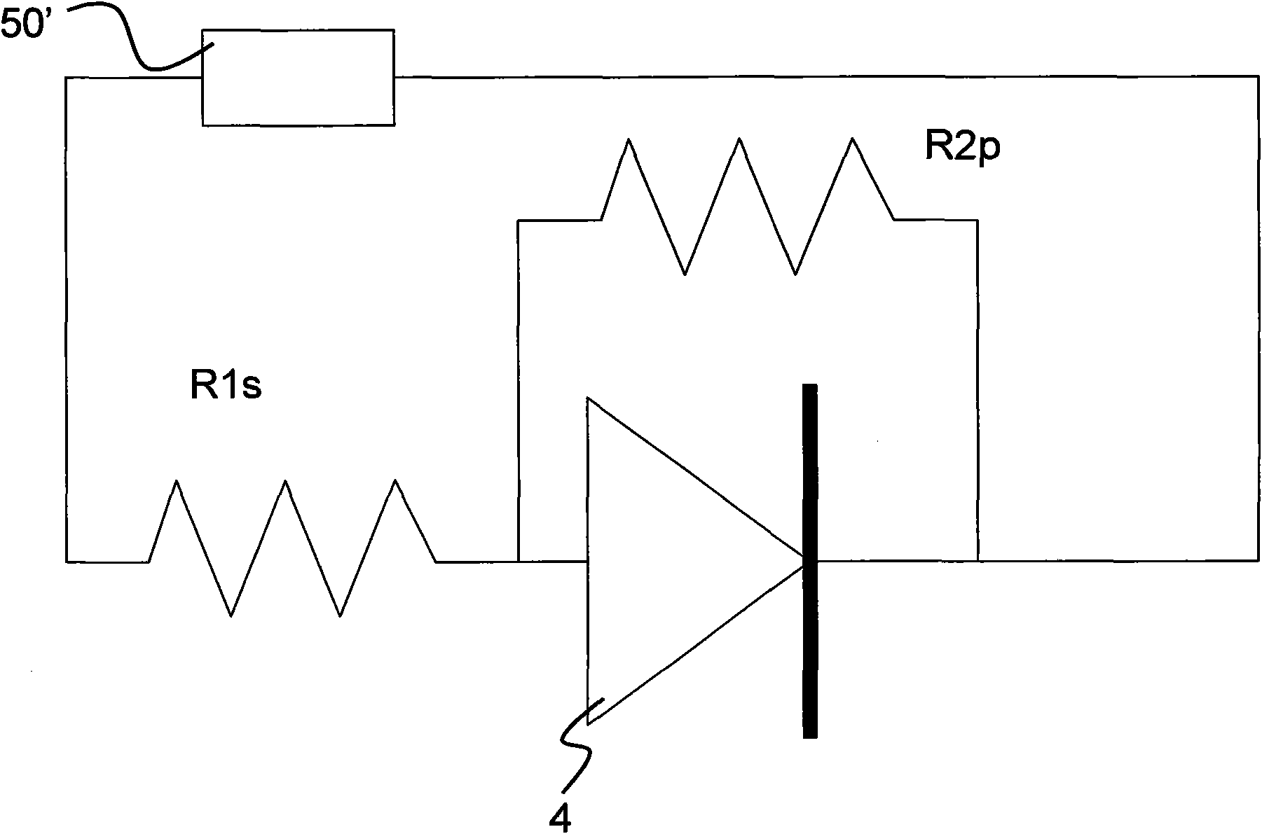
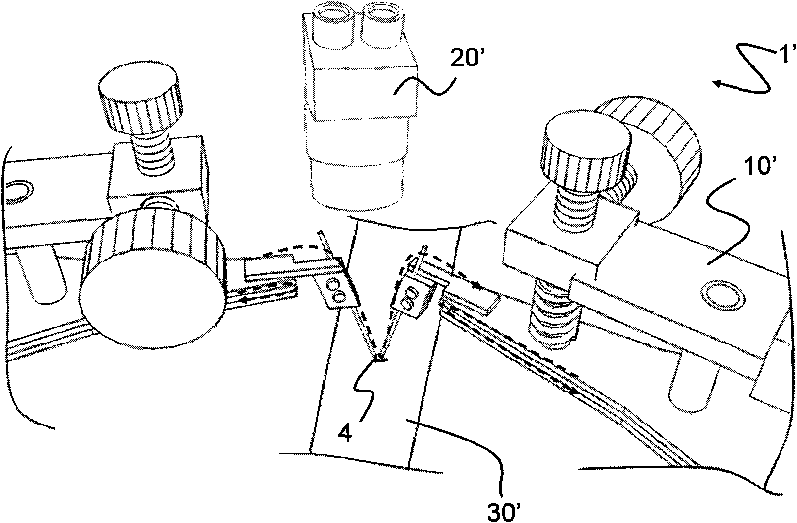
[0034] Such as figure 2 As shown, this is a schematic diagram of the simulated circuit of the grain to be tested. In this figure, the inherent minute resistance of the conductive circuit is represented by R1s, and the resistance of the insulating part used to isolate the circuit system from the rest of the components is represented by R2p. And when using the above-mentioned common structure detection, such as image 3 As shown, two groups of edge sensor...


PUM


Abstract

The invention relates to a semiconductor grain point measurement machine test method and a semiconductor grain point measurement machine. The method comprises the following steps of: adopting a group of point measurement machine conductive contact tested grains by the point measurement machine; sequentially exerting a small current test signal and a big current test signal to the tested grains; then receiving the current-voltage information returned by the tested grains; judging whether the deviation between the tested information and the given standard information exceeds a normal range or not till the deviation accumulatively exceeds the normal range for too many times; and stopping the grain detection and examining and repairing the machine after determining that the machine is in an abnormal state.

Description

【Technical field】 [0001] The invention relates to a machine inspection method, in particular to a semiconductor grain spot measurement machine inspection method and the machine. 【Background technique】 [0002] Since the advent of LED (light emitting diode), in addition to the advantages of energy saving, low temperature and long life compared with traditional light sources, the efficiency has been greatly improved with the improvement of the process, and the application fields have become more and more extensive. A single LED is used in small toys, handheld devices, and mobile phones, and multiple LEDs are used in lamps, automobiles, and traffic signs in daily life, making the manufacturing of LEDs and quality inspection at various stages necessary and even more important. [0003] In the automatic detection process of LED grains, the commonly used structures of common point measurement devices are as follows: figure 1 The shown edge sensor (edge ​​sensor) 10 uses a fine pr...

Claims


Application Information

Patent Timeline
Patent Type & Authority Applications(China)
IPC IPC(8): H01L21/66H01L21/00H01L33/00
Inventor 陶坚强陈正雄刘衍庆
Owner 致茂电子(苏州)有限公司
Why Eureka
Try Eureka