Plasma display panel driving method and plasma display device

A plasma and display panel technology, applied to static indicators, instruments, etc., can solve the problem of not being able to ensure the number of subfields

Inactive Publication Date: 2011-07-13
PANASONIC CORP
View PDF8 Cites 0 Cited by
  • Summary
  • Abstract
  • Description
  • Claims
  • Application Information

AI Technical Summary

Problems solved by technology

[0006] On the contrary, in the ADS method, it is necessary to set a sustain period in a period other than the write period, so when the time required for the write period becomes longer due to the high-definition of the plasma display panel, etc., there is a problem that it cannot ensure the quality of the image display. The problem of the sufficient number of subfields for

Method used


Image

  • Plasma display panel driving method and plasma display device
  • Plasma display panel driving method and plasma display device
  • Plasma display panel driving method and plasma display device

Examples


Embodiment approach 1

[0080] [Structure of Plasma Display Panel 10]

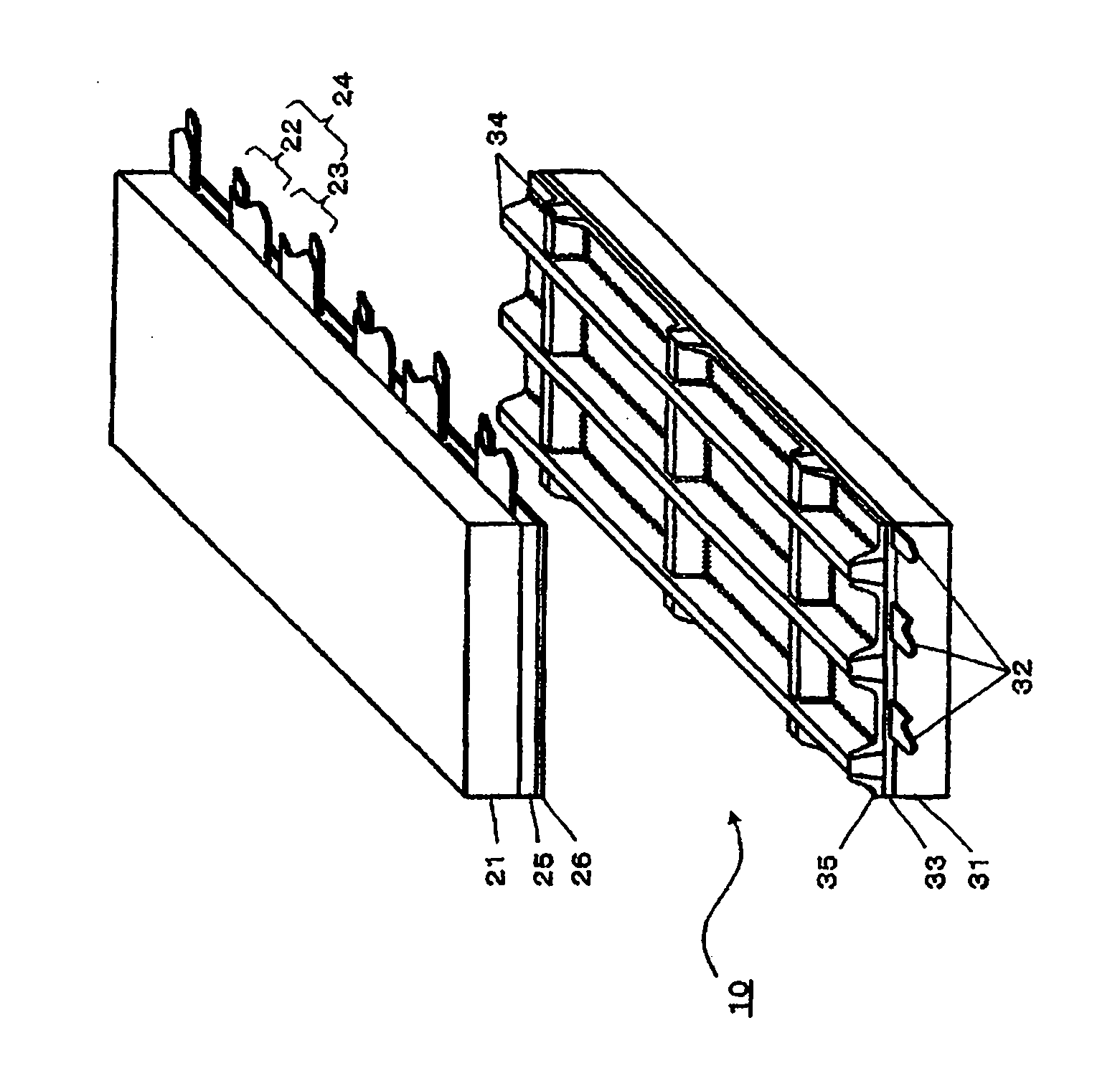
[0081] figure 1 It is an exploded perspective view of plasma display panel 10 of the plasma display device according to Embodiment 1 of the present invention. On front substrate 21 made of glass, a plurality of display electrode pairs 24 including scan electrodes 22 and sustain electrodes 23 are formed. Further, a dielectric layer 25 and a protective layer 26 are sequentially laminated on the front substrate 21 so as to cover the display electrode pairs 24 .

[0082]A plurality of data electrodes 32 are formed parallel to each other on rear substrate 31 . Further, on rear substrate 31 , dielectric layer 33 is formed so as to cover data electrodes 32 , and furthermore, lattice-shaped partition walls 34 are formed thereon. Then, phosphor layers 35 capable of emitting red, green, and blue light are provided in a space formed by the upper surface of dielectric layer 33 and the side surfaces of partition walls 34 .

[0083] Front ...

Embodiment approach 2

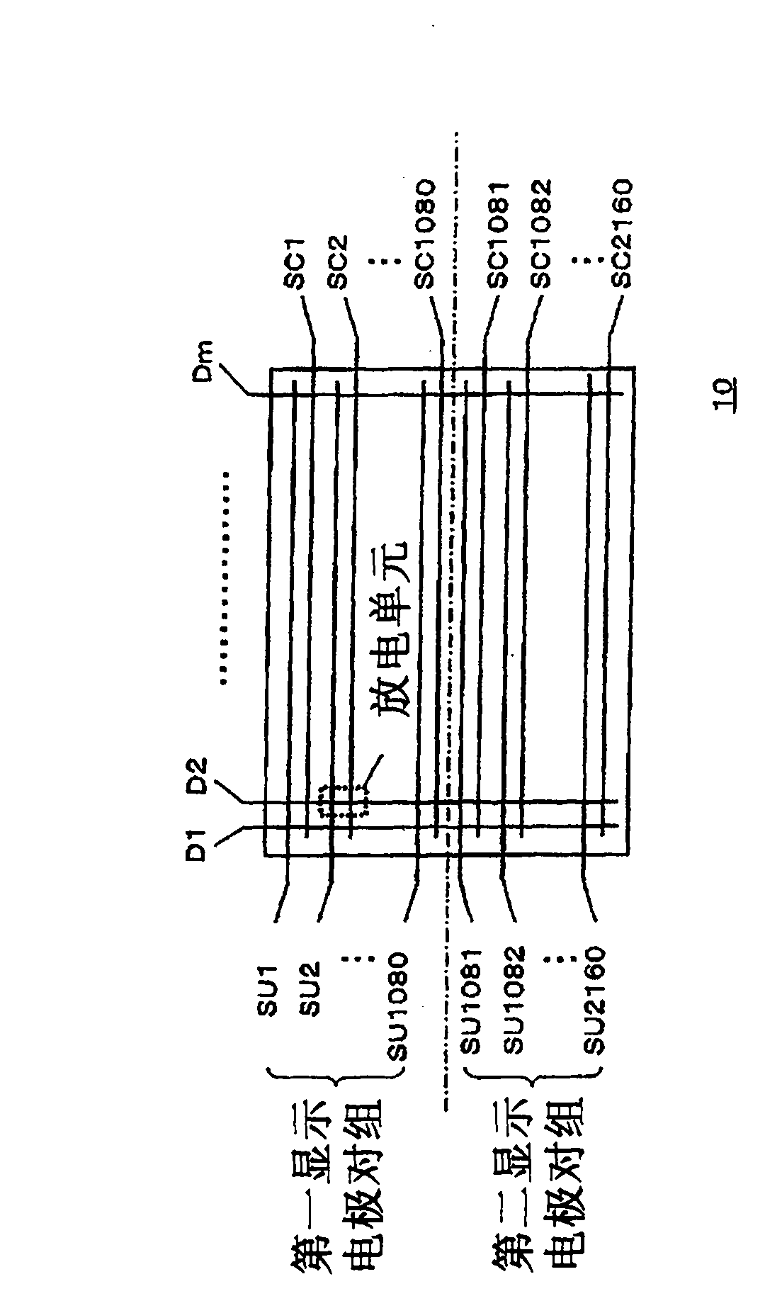
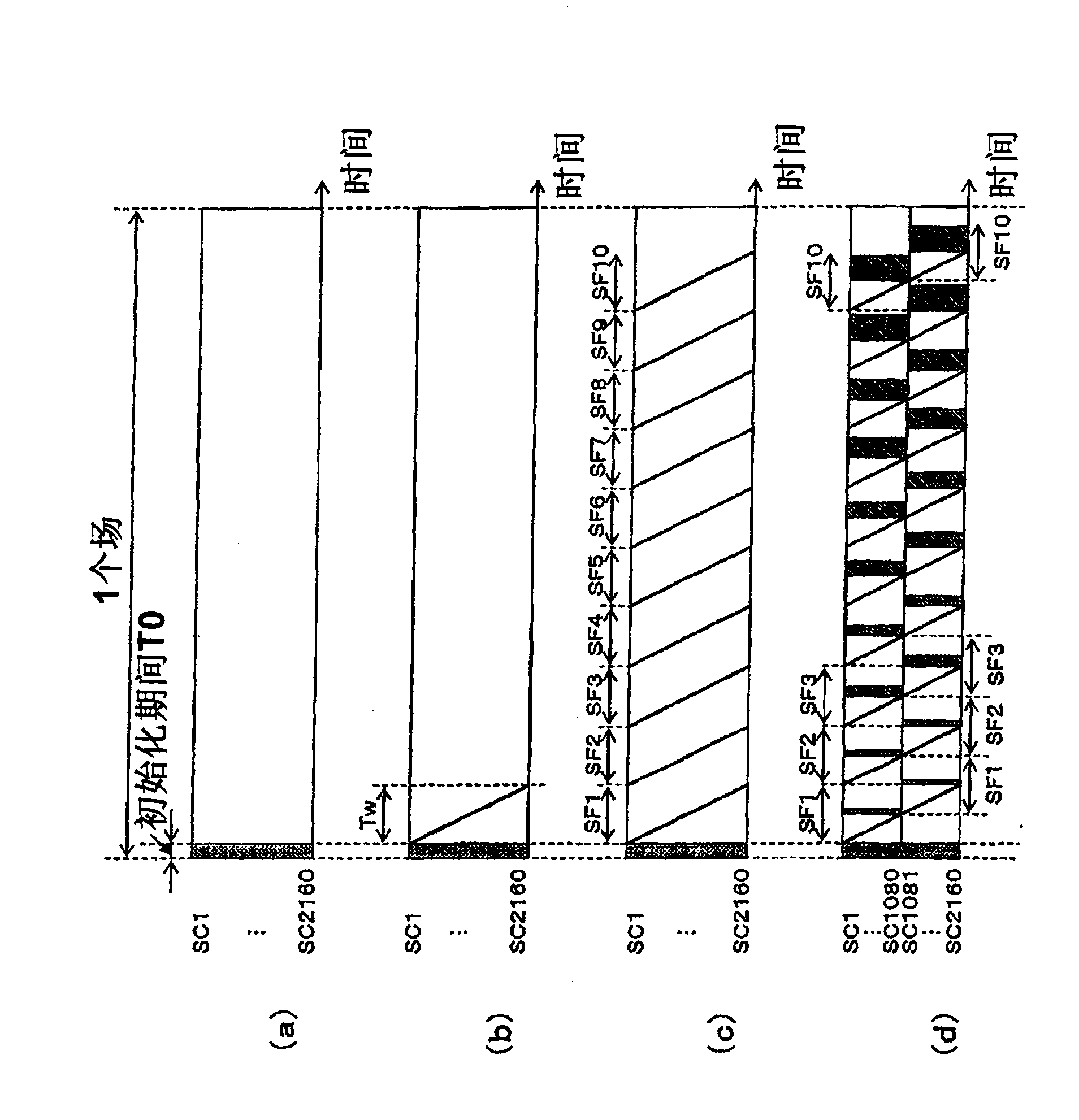
[0224] Figure 11 It is a diagram for explaining the subfield structure applied to the driving method of plasma display panel 10 in the second embodiment. which, with Figure 10 Similarly, the vertical axis represents scan electrodes SC1 to SC2160 , and the horizontal axis represents time. Also, a case where the wall voltage adjustment period is constituted by only the erasing period is shown. Furthermore, the timing of performing the write operation is indicated by a solid line, the sustain period is indicated by hatching from the upper right to the lower left, and the erasing period is indicated by hatching from the upper left to the lower right. The plasma display device in Embodiment 2, and Figure 5 The illustrated Embodiment 1 is the same as that described in Embodiment 1, so description thereof will be omitted.

[0225] The subfield structure of Embodiment 2, and Figure 10 The difference in the subfield structure of Embodiment 1 shown is that luminance weights, th...

Embodiment approach 3

[0233] Figure 12 It is a diagram for explaining the subfield structure applied to the driving method of plasma display panel 10 in the third embodiment. which, with Figure 10 Similarly, the vertical axis represents scan electrodes SC1 to SC2160 , and the horizontal axis represents time. Also, a case where the wall voltage adjustment period is constituted by only the erasing period is shown. Furthermore, the timing of performing the write operation is indicated by a solid line, the sustain period is indicated by hatching from the upper right to the lower left, and the erasing period is indicated by hatching from the upper left to the lower right. The plasma display device in Embodiment 3 is the same as that described in Embodiment 1, so description thereof will be omitted.

[0234] Figure 12 In , the subfield structure in which the subfield with the highest lighting rate is subfield SF8 is shown. The subfield with the highest lighting rate in one field has the largest n...


PUM


Abstract

Disclosed are a plasma display panel driving method and a plasma display device. In the plasma display panel driving method, a plurality of display electrode pairs is divided into a plurality of display electrode pair groups, and one field is divided into a plurality of subfields. The length of a sustainment period and the length of an erase period are compared with each other. In the case where the sustainment period is longer than the erase period, a sustainment discharge and an erase discharge are performed for each display electrode pair group. In the case where the sustainment period is shorter than the erase period, the sustainment discharge and the erase discharge are performed in synchronization with each other among the display electrode pair groups. Further, in a subfield having the largest luminance weight or in a subfield having the largest light rate, the sustainment discharge and the erase discharge are performed in synchronization with each other among the display electrode pair groups.

Description

technical field [0001] The present invention relates to a driving method of a plasma display panel and a plasma display device using the same. Background technique [0002] In a typical AC surface discharge type panel that is a plasma display panel, a plurality of discharge cells are formed between a front substrate and a rear substrate that are arranged to face each other. [0003] Multiple pairs of display electrodes consisting of scan electrodes and sustain electrodes are formed parallel to each other on the front substrate, and multiple data electrodes are formed parallel to each other on the rear substrate. Then, the front substrate and the rear substrate are arranged and sealed in such a way that the display electrode pairs intersect the data electrodes three-dimensionally, and the discharge gas is sealed in the internal discharge space. Here, the discharge cells are formed at portions where the display electrode pairs face the data electrodes. [0004] As a method o...

Claims


Application Information

Patent Timeline
Patent Type & Authority Applications(China)
IPC IPC(8): G09G3/28G09G3/20G09G3/288G09G3/291G09G3/292G09G3/293G09G3/294G09G3/296G09G3/298
CPCG09G3/294G09G3/2965G09G3/293G09G3/2927G09G3/2022G09G2310/0218G09G2310/0216G09G3/292
Inventor 中田秀树牧野弘康新井康弘若林俊一小南智井土真澄松下纯子
Owner PANASONIC CORP
Why Eureka
Try Eureka