Semiconductor device
A semiconductor and device technology, applied in the field of semiconductor devices, can solve the problems of reduced on-resistance and drift resistance, and achieve the effects of reducing electric field concentration, improving breakdown voltage and breakdown resistance
- Summary
- Abstract
- Description
- Claims
- Application Information
AI Technical Summary
Problems solved by technology
Method used
Image

Examples
no. 1 example
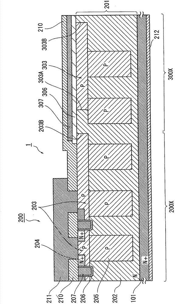
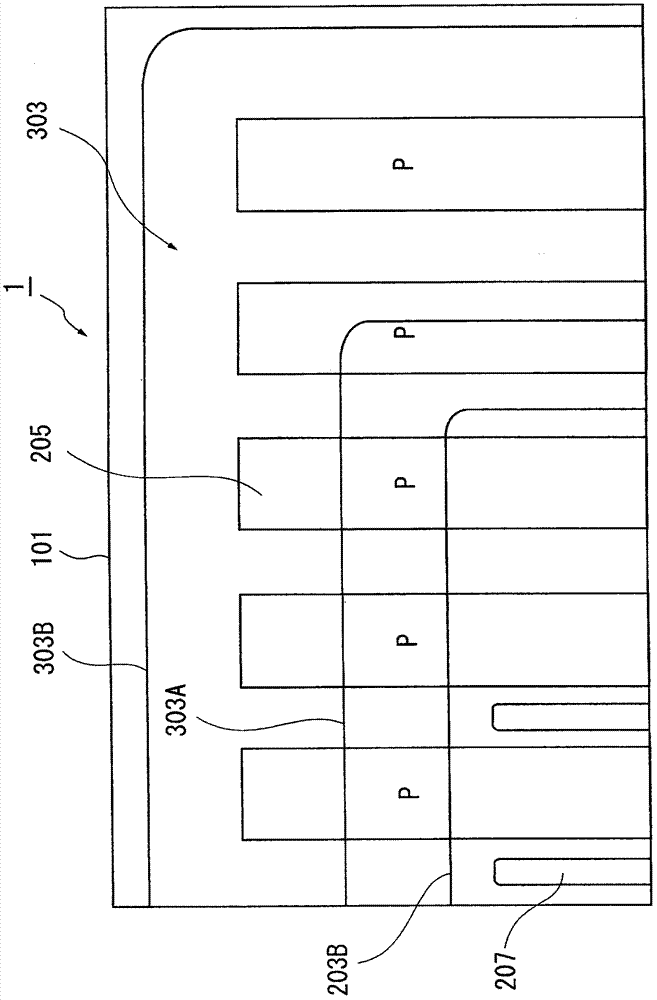
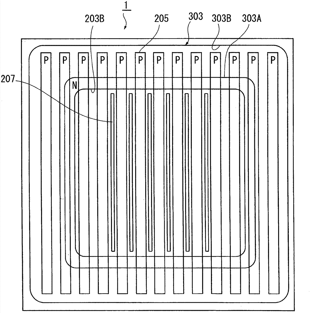
[0054] An exemplary structure of a semiconductor device according to a first embodiment of the present invention will be described with reference to the drawings. figure 1 is a cross-sectional view showing a main part of the semiconductor device according to the first embodiment. Figure 2A is a plan view of the main part of the semiconductor device. Figure 2B is an overall plan view of the semiconductor device. For clarity of description, the scale and position of each component are appropriately changed and are different from actual ones.
[0055] The semiconductor device 1 of the first embodiment has a structure in which at least one vertical power MOSFET (transistor element) 200 having a super junction (SJ) structure is formed on a first conductivity type semiconductor substrate 101 . In the first embodiment, a plurality of MOSFETs 200 are formed on a single semiconductor substrate 101 . A region in which a plurality of MOSFETs 200 are formed is called an element forma...
no. 2 example
[0108] The structure of a semiconductor device according to a second embodiment of the present invention will be described with reference to the drawings. Figure 5 is a cross-sectional view showing a main part of the semiconductor device of the second embodiment. The same components as those of the first embodiment are denoted by the same reference numerals, and descriptions thereof are omitted.
[0109] The basic structure of the semiconductor device 2 of the second embodiment is similar to that of the semiconductor device of the first embodiment. In the second embodiment, the second conductivity type annular diffusion region 303 in the peripheral region 300X is divided into a plurality of regions with spaces therebetween. In the second embodiment, the second conductivity type annular diffusion region 303 is divided into two regions 303P1 (inside) and 304P2 (outside).
[0110] In the second embodiment, the positions of the innermost end 303A and the outermost end 303B of t...
no. 3 example
[0114] The structure of a semiconductor device according to a third embodiment of the present invention will be described with reference to the drawings. Figure 6 is a cross-sectional view showing a main part of a semiconductor device according to a third embodiment. The same components as those of the first embodiment are denoted by the same reference numerals, and descriptions thereof are omitted.
[0115] The basic structure of the semiconductor device 3 of the third embodiment is similar to that of the semiconductor device of the first embodiment. According to the third embodiment, in the element formation region 200X, the second conductivity type base region 203 and the second conductivity type columnar region 205 are spaced apart from each other when viewed in cross section. The second conductivity type base region 203 of the element formation region 200X and the second conductivity type annular diffusion region 303 of the peripheral region 300X are preferably formed i...
PUM
 Abstract
Description
Claims
Application Information
 - R&D
- Intellectual Property
- Life Sciences
- Materials
- Tech Scout
- Unparalleled Data Quality
- Higher Quality Content
- 60% Fewer Hallucinations
Browse by: Latest US Patents, China's latest patents, Technical Efficacy Thesaurus, Application Domain, Technology Topic, Popular Technical Reports.
© 2025 PatSnap. All rights reserved.Legal|Privacy policy|Modern Slavery Act Transparency Statement|Sitemap|About US| Contact US: help@patsnap.com