Method for realizing onboard programming of flash chip and equipment thereof

A flash memory and chip technology, applied in the field of communication, can solve the problems of limited device selection, high cost, and many FPGA pins

Inactive Publication Date: 2011-11-23
DATANG MOBILE COMM EQUIP CO LTD
View PDF3 Cites 2 Cited by
  • Summary
  • Abstract
  • Description
  • Claims
  • Application Information

AI Technical Summary

Problems solved by technology

The boundary scan method requires the circuit board hardware design to support the boundary scan function, and the selection of devices is limited; it is also necessary to insert a boundary scan control card into the PC, and support the driver of the boundary scan control card and software for various operations. Requires special design and high cost
The parallel port programming method needs to lead out a parallel port on the circuit board. It is necessary to add a special program for the design of the circuit board and the control of the parallel port to complete the command sending and file transfer functions, and it takes up more FPGA pins.

Method used


Image

  • Method for realizing onboard programming of flash chip and equipment thereof
  • Method for realizing onboard programming of flash chip and equipment thereof
  • Method for realizing onboard programming of flash chip and equipment thereof

Examples


Embodiment Construction

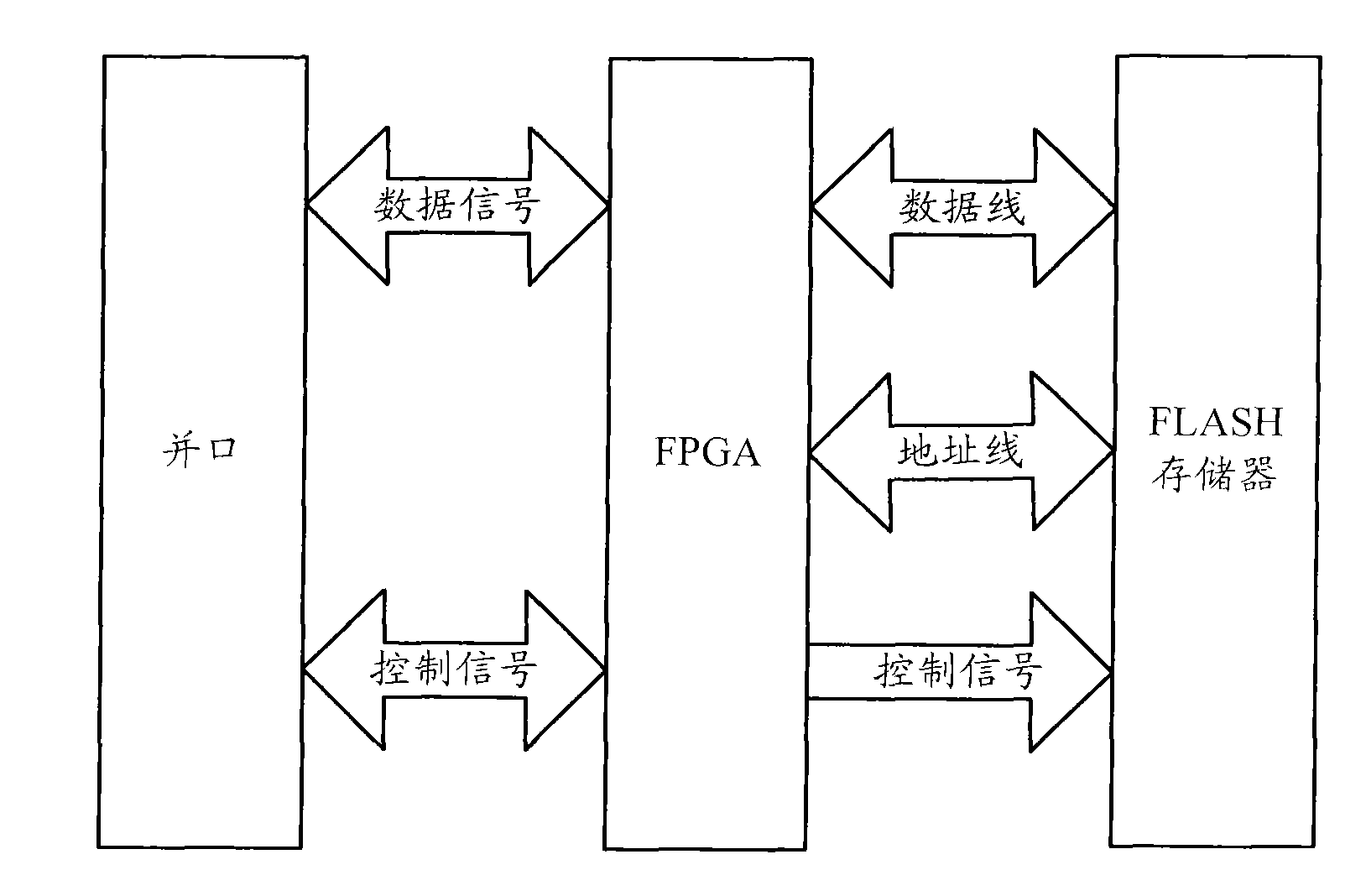
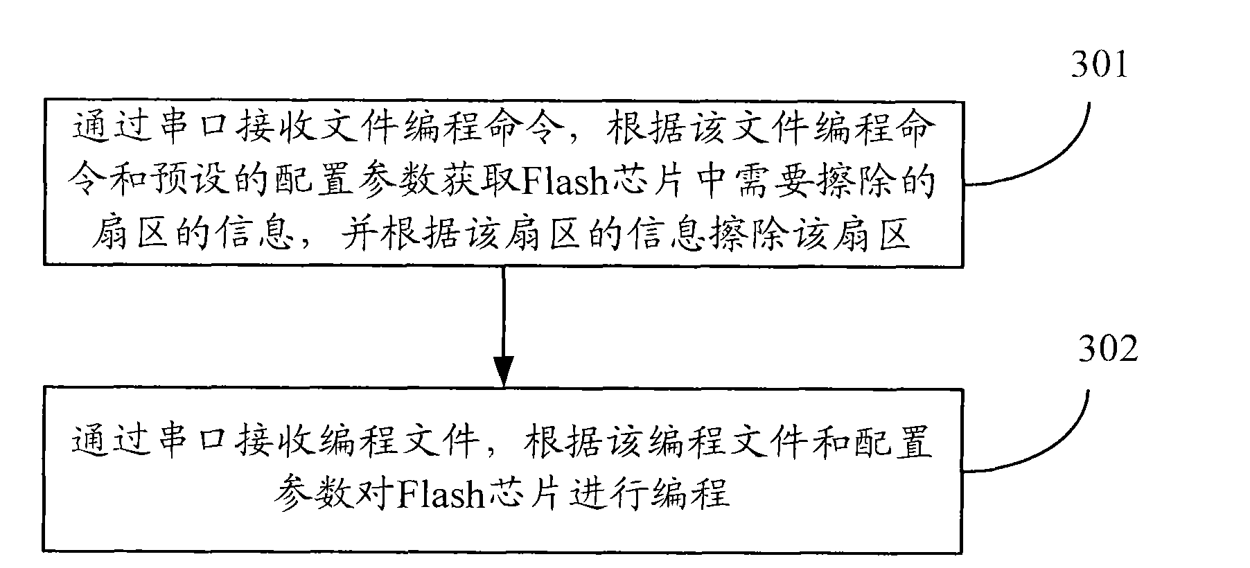
[0046] In order to solve the programming problem of the Flash chip welded on the circuit board, the embodiment of the present invention can complete the programming of the Flash chip when the Flash chip is empty (there is no program in the Flash chip) or the program in the Flash chip is destroyed. The programming data is transmitted from the PC to the circuit board through the RS232 serial port. The transmission of the programming data is carried out through the Xmodem protocol. The PC side only needs to start the standard component "HyperTerminal" of Windows.

[0047] Among them, RS232 is a widely used serial communication port standard, referred to as serial port standard; Xmodem protocol is an asynchronous file transfer protocol widely used in personal computer communications using dial-up modems, and supports serial port for file transfer. Data is transmitted in 128-byte blocks, and each block can use a checksum process for error detection. If the receiver's checksum for a ...


PUM


Abstract

The embodiment of the invention discloses a method for realizing the onboard programming of a flash chip and equipment thereof. The method comprises the steps of: receiving a file programming command through a serial port, according to the file programming command and preset configuration parameters, acquiring information about the sector needing to be erased in the flash chip, and erasing the sector on the basis of the sector information; receiving a programming file through the serial port, programming the flash chip according to the programming file and the configuration parameters. The embodiment of the invention simplifies the hardware design of a single board.

Description

technical field [0001] The invention relates to the field of communication technology, in particular to a method and device for realizing on-board programming of a flash memory chip. Background technique [0002] In the circuit board design of electronic equipment, various processors are used. The program code run by the processor is stored in the Flash (flash memory) chip of the circuit board. The Flash chip has the ability to maintain data after power failure. Programming and data reading can be performed with special timing. However, most Flash chips will be soldered to the circuit board at one time, which makes it difficult to program the Flash chip. You cannot use a traditional programmer to program the chip, but use the program in the Flash chip to program itself. . However, when the program in the Flash chip is destroyed or the Flash chip is empty, the Flash chip cannot program itself, and other methods must be used to complete the programming of the Flash chip. ...

Claims


Application Information

Patent Timeline
Patent Type & Authority Applications(China)
IPC IPC(8): G11C16/10G11C16/16
Inventor 张巧宁
Owner DATANG MOBILE COMM EQUIP CO LTD
Why Eureka
Try Eureka