Liquid crystal display panel and production method thereof

A technology for liquid crystal display panels and substrates, which is used in semiconductor/solid-state device manufacturing, optics, instruments, etc., and can solve problems such as poor capacitance effect and decreased storage capacitance value.

Inactive Publication Date: 2014-03-12
DONGGUAN MASSTOP LIQUID CRYSTAL DISPLAY +1
View PDF5 Cites 0 Cited by
  • Summary
  • Abstract
  • Description
  • Claims
  • Application Information

AI Technical Summary

Problems solved by technology

As a result, the capacitive effect between the capacitive electrode and the pixel electrode is not good, and the storage capacitance value decreases

Method used


Image

  • Liquid crystal display panel and production method thereof
  • Liquid crystal display panel and production method thereof
  • Liquid crystal display panel and production method thereof

Examples


no. 1 example

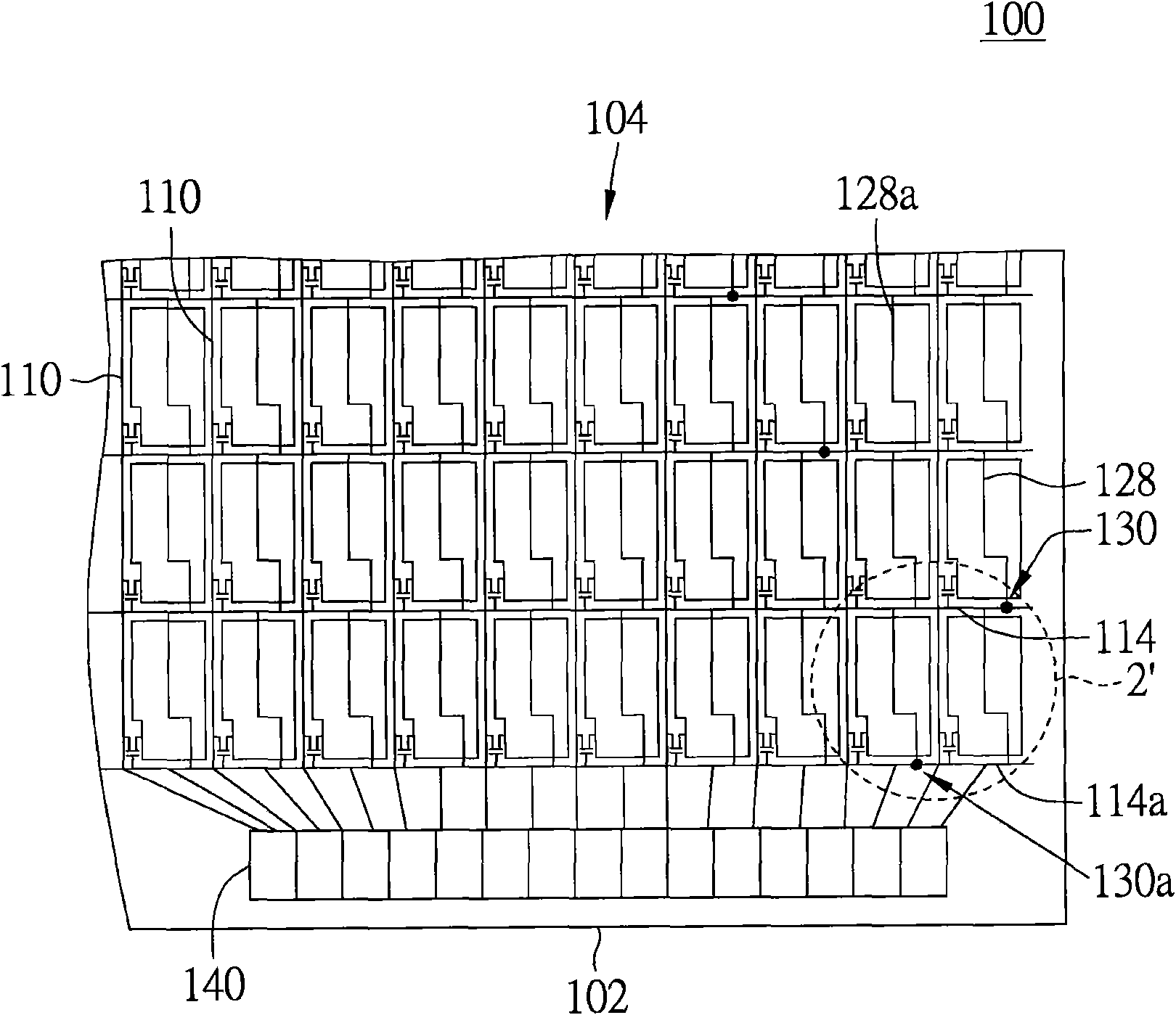
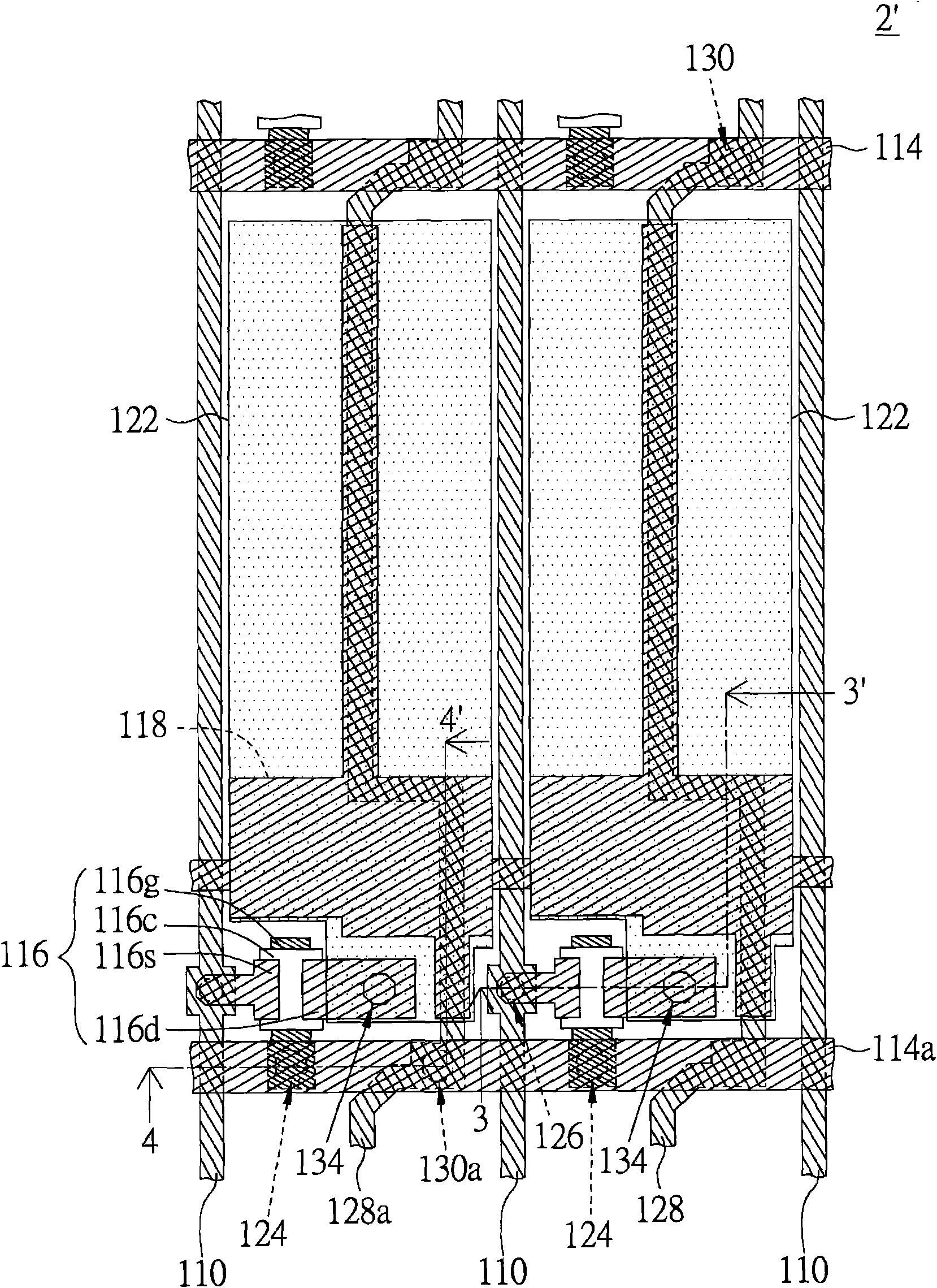
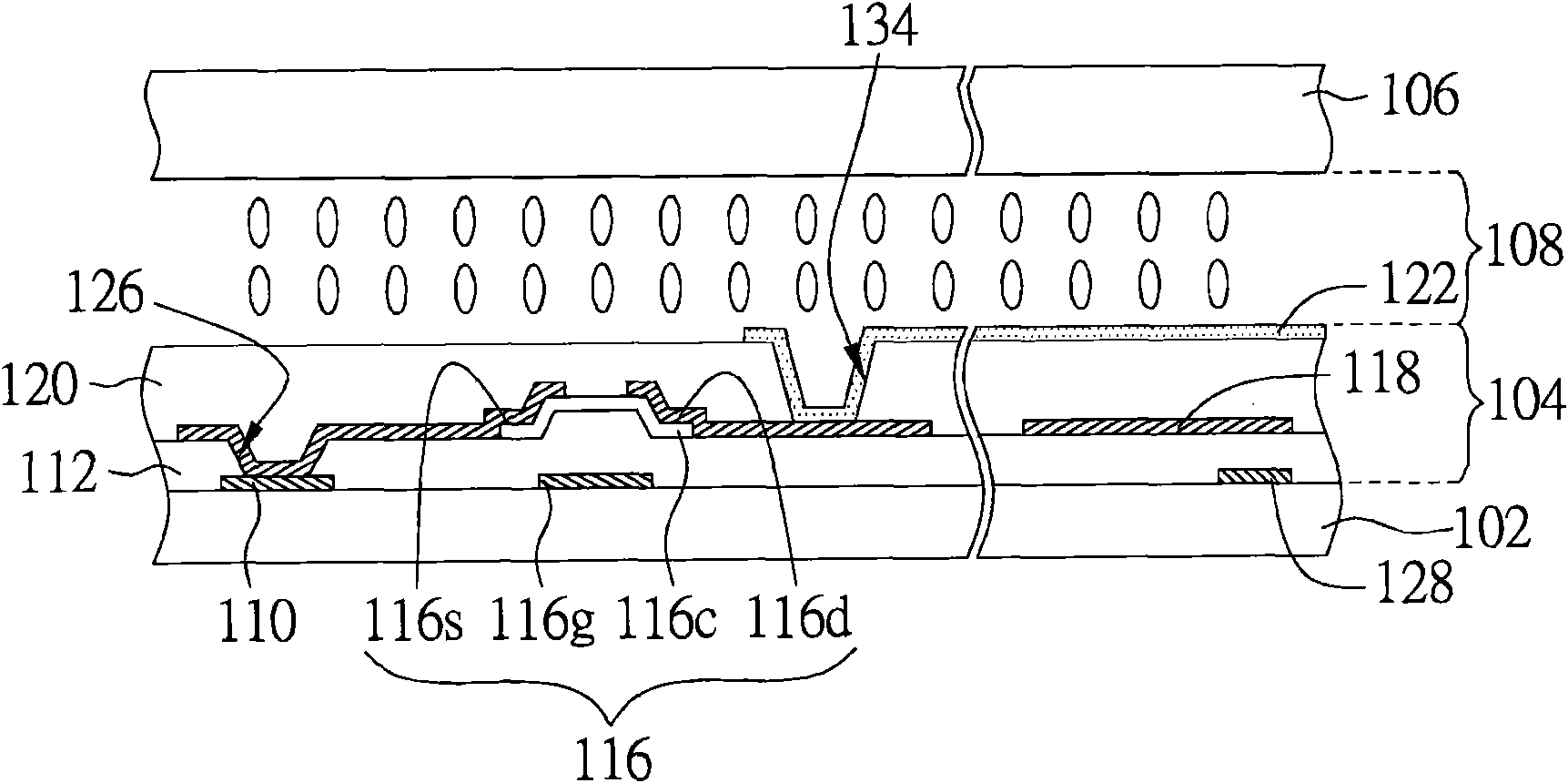
[0044] Please refer to Figure 1 to Figure 3 , figure 1 A partial schematic diagram of a liquid crystal display panel according to a first embodiment of the present invention is shown, figure 2 draw figure 1 The enlarged schematic diagram of the middle part 2', image 3 draw figure 2 Sectional view of 3-3' in the middle direction. like figure 1 , the liquid crystal display panel 100 includes a first substrate 102, a pixel array 104, and a second substrate 106 (shown in image 3 ), liquid crystal layer 108 (shown in image 3 ) and drive circuit 140. The liquid crystal layer 108 is disposed between the first substrate 102 and the second substrate 106 .

[0045] Please also refer to figure 2 and image 3 The pixel array 104 is formed on the first substrate 102 and includes several data lines 110, several scan lines 114, several active elements 116, several capacitor electrodes 118, several pixel electrodes 122 and several gate lines 128 . Among them, adjacent capac...

no. 2 example

[0067] Please refer to Figure 7 , which shows a partial schematic diagram of a liquid crystal display panel according to a second embodiment of the present invention. The parts in the second embodiment that are the same as those in the first embodiment use the same reference numerals, which will not be repeated here. The difference between the liquid crystal display panel 200 of the second embodiment and the liquid crystal display panel 100 of the first embodiment is that the liquid crystal display panel 200 does not include the gate lines 128 and the scan line openings 130 .

[0068] Please refer to Figure 8 , which shows Figure 7 Sectional view in the middle direction 8-8'. The liquid crystal display panel 200 includes a first substrate 102 , a pixel array 204 , a second substrate 106 and a liquid crystal layer 108 .

[0069] The pixel array 204 includes several data lines 210 , a first insulating layer 212 , several scan lines 214 , several active elements 216 , seve...


PUM


Abstract

The invention discloses a liquid crystal display panel and a production method thereof. The liquid crystal display panel comprises a pixel array. The pixel array comprises a plurality of data lines, a first insulating layer, a plurality of scanning lines, a plurality of active elements, a plurality of capacitive electrodes, a second insulating layer and a plurality of pixel electrodes. The first insulating layer covers the data lines and is provided with a plurality of grid holes and a plurality of source holes. The scanning lines are formed on the first insulating layer. Each active element comprises a grid, a source and a drain. The sources, the grids and the capacitive electrodes are formed on the first insulating layer. The second insulating layer covers the capacitive electrodes, the sources and the drains. The pixel elements correspond to the capacitive electrodes and are formed on the second insulating layer. The scanning lines are electrically connected with the corresponding grids via the corresponding grid holes, and the data lines are electrically connected with the corresponding sources via the corresponding source holes.

Description

technical field [0001] The invention relates to a liquid crystal display panel and a manufacturing method thereof, in particular to a liquid crystal display panel in which data lines and gates are arranged on the same layer and a manufacturing method thereof. Background technique [0002] At present, in the manufacturing technology of liquid crystal display, there are several technologies that can meet the requirement of wide viewing angle, such as twisted nematic liquid crystal (TN) plus wide viewing film (Wide Viewing Film), in-plane switching (In-plane Switching, IPS) ) liquid crystal display, fringe field switching (Fringe Field Switching) liquid crystal display and multi-domain vertical alignment liquid crystal display. [0003] In order to connect the pixel array in the liquid crystal display panel to the driving circuit, some lines for transmitting signals are arranged around the display area in the conventional design to avoid further limiting the display aperture ra...

Claims


Application Information

Patent Timeline
Patent Type & Authority Patents(China)
IPC IPC(8): G02F1/1362G02F1/1333H01L27/02H01L21/77
Inventor 叶政谚林仲凯
Owner DONGGUAN MASSTOP LIQUID CRYSTAL DISPLAY
Why Eureka
Try Eureka