

Touch control panel
A touch panel and touch technology, which is applied to instruments, electrical digital data processing, and data processing input/output process, etc. rate effect
- Summary
- Abstract
- Description
- Claims
- Application Information
AI Technical Summary
Problems solved by technology
Method used
Image

Examples
no. 1 example
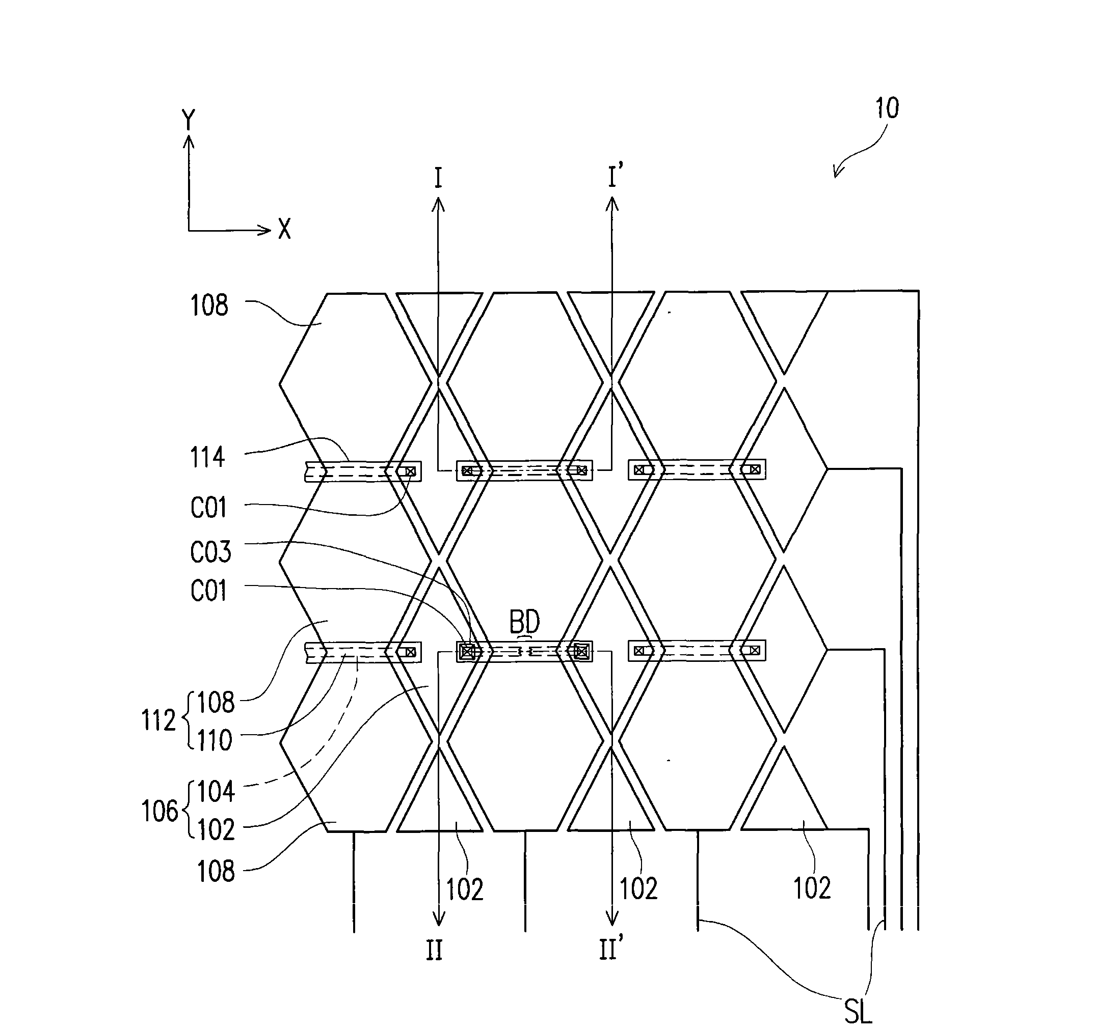
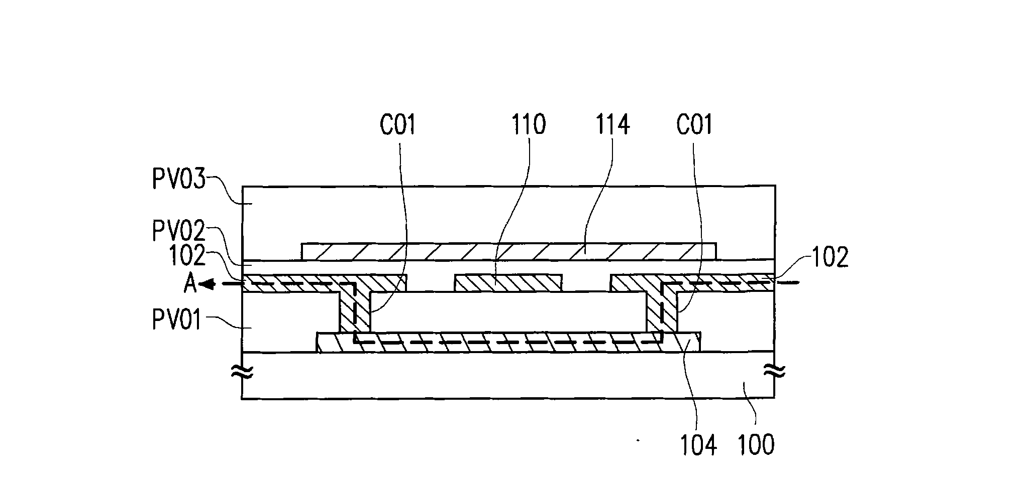
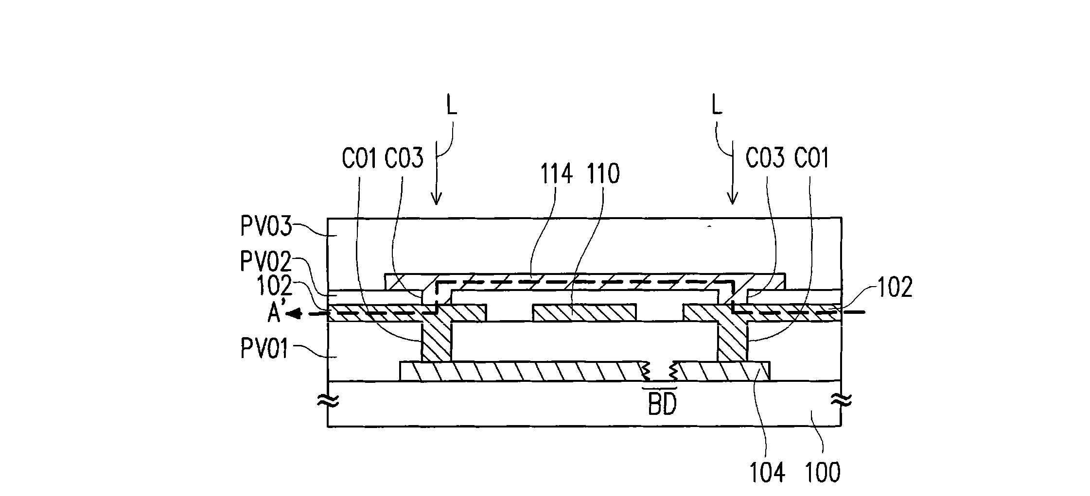
[0058] figure 1 is a partial top view diagram of the touch panel according to the first embodiment of the present invention, Figure 2A and Figure 2B for figure 1 The partial cross-sectional schematic diagram of the touch panel, where Figure 2A corresponds to figure 1 at the I-I' profile line, and Figure 2B corresponds to figure 1 at the II-II' section line. Please also refer to figure 1 , Figure 2A as well as Figure 2B The touch panel 10 of this embodiment includes a plurality of first touch series 106 , a plurality of second touch series 112 , a first insulating layer PV01 , a plurality of conductive patterns 114 and a second insulating layer PV02 .
[0059] Please refer to figure 1 , the first touch series 106 and the second touch series 112 are disposed on the substrate 100 , wherein the first touch series 106 extends in a first direction, and the second touch series 112 extends in a second direction. In this embodiment, the first and second directions are ...
no. 2 example
[0080] Figure 6 is a schematic partial top view of a touch panel according to a second embodiment of the present invention, Figure 7A and Figure 7B for Figure 6 The partial cross-sectional schematic diagram of the touch panel, where Figure 7A corresponds to Figure 6 at the III-III’ section line, and Figure 7B corresponds to Figure 6 The IV-IV' section line. In this embodiment, the same elements as those of the first embodiment described above are denoted by the same symbols, and descriptions thereof will not be repeated.
[0081] Please also refer to Figure 6 , Figure 7A as well as Figure 7B , the touch panel of this embodiment includes a plurality of first touch series 106 , a plurality of second touch series 112 , insulating layers PV01 , PV02 , PV03 and a plurality of conductive patterns 202 . In this embodiment, the first touch series 106 and the second touch series 112 are the same as the above-mentioned first embodiment. Similarly, the first insulat...
PUM
 Abstract
Description
Claims
Application Information