Saw device and method of manufacture

a technology of a saw and a manufacturing method, which is applied in the direction of vacuum evaporation coating, sputtering coating, coating, etc., can solve the problems of increasing performance and yield, affecting the yield and affecting the performance of the device, so as to achieve the effect of increasing the effective distance between the target and the substrate and maintaining the devi

Active Publication Date: 2019-08-29
SPTS TECH LTD
View PDF0 Cites 2 Cited by
  • Summary
  • Abstract
  • Description
  • Claims
  • Application Information

AI Technical Summary

Benefits of technology

[0021]An important aspect of high volume production of filter devices is maintaining device yield and performance across the lifetime of the target. In a sputtering apparatus, the effective distance between the target and the substrate may increase as the target is depleted. Furthermore, depletion of the target may be non-uniform across the surface of the target. This can lead to a drift in the silicon oxide film properties of SAW

Problems solved by technology

In particular, it has been determined that surface roughness of the silicon oxide layer correlates directly with non-uniformity of the frequency distribution within the devic

Method used


Image

  • Saw device and method of manufacture
  • Saw device and method of manufacture
  • Saw device and method of manufacture

Examples


Embodiment Construction

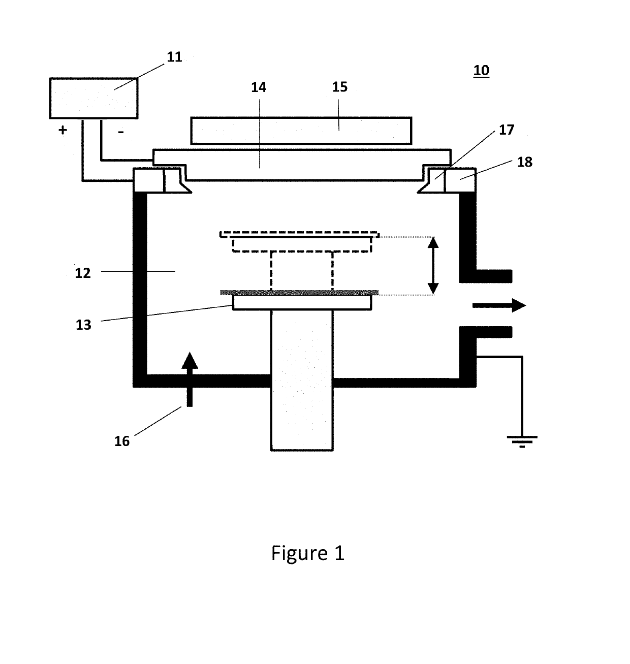
[0060]FIG. 1 shows a typical apparatus 10 for carrying out the invention in the form of a pulsed DC magnetron reactive sputtering arrangement. The apparatus includes a vacuum chamber 12 within which is located a wafer platen 13. An upper portion of the chamber 12 includes a circular target 14, which can be formed from silicon or silicon dioxide. A pulsed DC power supply 11 is provided to apply pulsed DC power to the target 14, which acts as a cathode. The apparatus 10 further comprises an anode 17 in the form of an annular ring made of a metal (typically aluminium or stainless steel) which surrounds the perimeter of the target 14. The anode 17 is supported by an insulating part 18 (e.g. a ceramic insulator) to avoid it touching the grounded chamber 12 and to keep it isolated from the target 14 which is situated above it. A magnetron 15 of known type is located behind (above) the target 14.

[0061]In use, the platen 13 supports a substrate, typically a wafer, in opposition to the targe...


PUM

PropertyMeasurementUnit
Fractionaaaaaaaaaa
Fractionaaaaaaaaaa
Fractionaaaaaaaaaa

Abstract

A method of reducing non-uniformity in the resonance frequencies of a surface acoustic wave (SAW) device, the SAW device comprising a silicon oxide layer comprising an oxide of silicon deposited over interdigital transducers on a piezoelectric substrate by reactive sputtering. The method comprises positioning a piezoelectric substrate having interdigital transducers on a substrate support, then depositing a silicon oxide layer comprising an oxide of silicon over the piezoelectric substrate and the interdigital transducers to form a SAW device. The substrate support is positioned relative to a sputtering target so that the silicon oxide layer of the SAW device has an arithmetic mean surface roughness (Ra) of 11 angstroms or less.

Description

[0001]The present invention relates to surface acoustic wave (SAW) devices, e.g. temperature-compensated SAW devices (TC-SAW) and methods of manufacturing a SAW device.BACKGROUND[0002]Surface acoustic wave (SAW) devices, e.g. filters, are a critical component in the RF front end of devices such as smartphones and tablets. SAW devices provide cheap and reliable RF filtering with high selectivity, low power and small footprint. A modern, multi-band, smartphone may contain 10 or more SAW devices and this number is only set to increase with every new smartphone release. As demand for SAW devices increases, production aspects of the constituent films require even tighter control in order to improve filter performance, maximize yield and reduce unit cost.[0003]A typical SAW device comprises a polished piezoelectric crystal substrate, usually lithium niobate (LiNbO3) or lithium tantalate (LiTaO3), on which is deposited an arrangement of interdigital transducers (IDTs). The IDTs comprise in...

Claims


Application Information

Patent Timeline
IPC IPC(8): H03H3/10H03H9/02H03H9/25H03H9/64H03H9/145C23C14/35C23C14/34C23C14/08
CPCH03H3/10H03H9/02559H03H9/02834H03H9/25C23C14/08H03H9/14544C23C14/35C23C14/3485H03H9/6489H03H9/64H10N30/883H10N30/02H03H2003/0442C23C14/10C23C14/345C23C14/0036C23C14/545H03H3/08H03H9/02H03H9/145H10N30/88
Inventor HYNDMAN, RHONDABURGESS, STEVE
Owner SPTS TECH LTD
Why Eureka
Try Eureka