Integrated overdrive and overvoltage protection device
A protection device, overvoltage technology, applied in the direction of emergency protection circuit device for limiting overcurrent/overvoltage, protection reacting to overvoltage, emergency protection circuit device, etc., can solve problems such as damage
Active Publication Date: 2012-09-19
FAIRCHILD SEMICON CORP
5 Cites 4 Cited by
AI-Extracted Technical Summary
Problems solved by technology
Mismatched and/or independently operating components can lead to various irregular failure ...
Method used
[0041] Since the overcurrent protection part 110, the control circuit 120 and/or the overvoltage protection part 130 can be integrated into a single component, assembly can be simplified and production costs can be reduced. In some embodiments, the overcurrent protection portion 110, the control circuit 120, and/or the overvoltage protection portion 130 may be integrated into a single component (ie, the input power protection device 100), such that separate overcurrent protection devices and overvoltage protection devices Installation into a computing device (eg, such as computing device 10) may not be necessary. Instead, overcurrent protection and overvoltage protection may be provided by the input power protection device 100 , which includes both the overcurrent protection portion 110 and the overvoltage protection portion 130 . In some embodiments, circuit board space may be allocated more efficiently by using input power protection device 100 , which may be a single component, than if multiple separate components were used to implement overcurrent protection and overvoltage protection. In some embodiments, heat transfer between component...
Abstract
In one general aspect, an apparatus can include an overcurrent protection device. The apparatus can include an overvoltage protection device coupled to the overcurrent protection device and configured to cause the overcurrent protection device to decrease a current through the overvoltage protection device after a breakdown voltage of the overvoltage protection device increases in response to heat.
Application Domain
TransistorElectronic switching +2
Technology Topic
EngineeringOvervoltage +2
Image
Examples
- Experimental program(1)
Example Embodiment
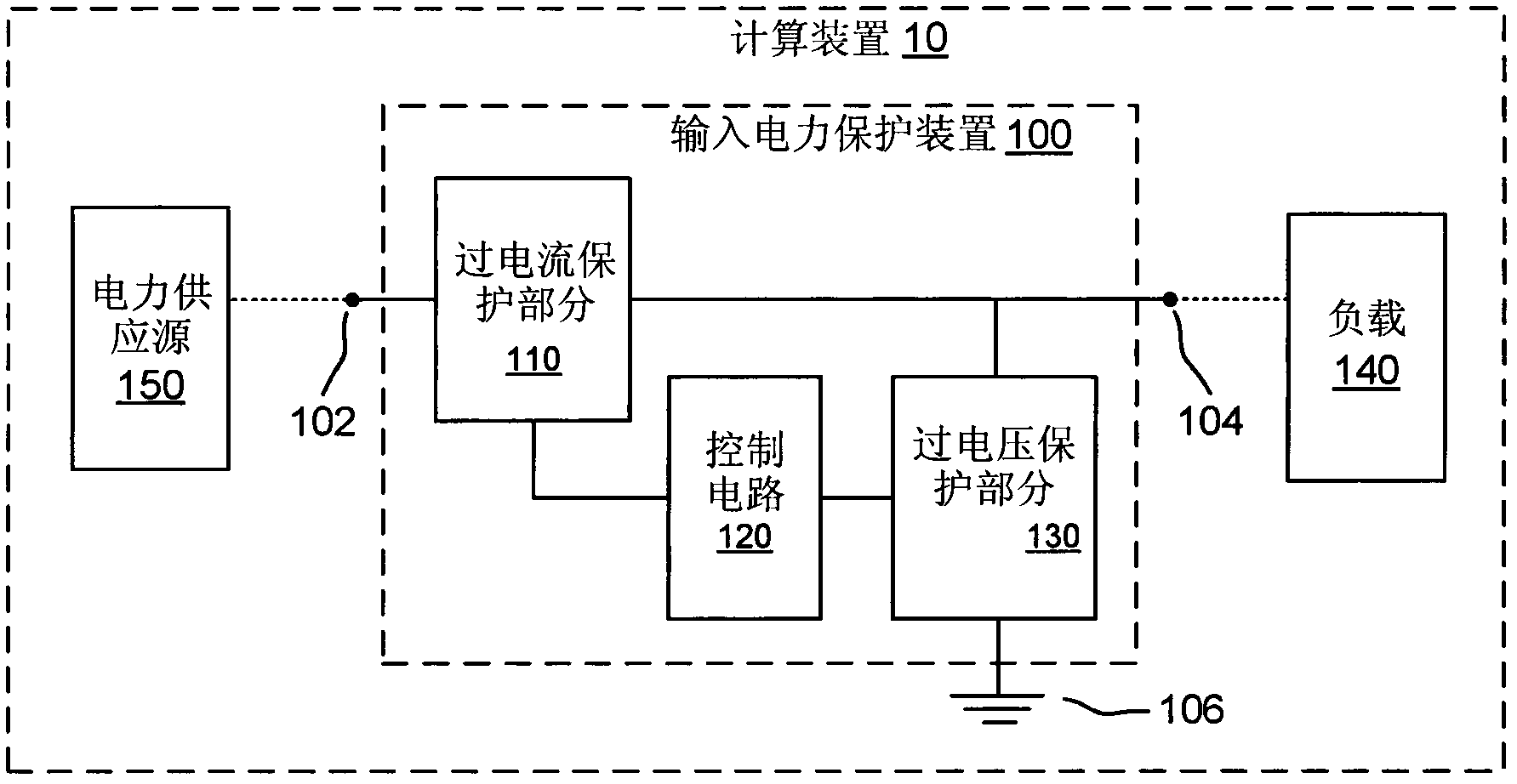
[0023] figure 1 is a block diagram illustrating the input power protection device 100 . like figure 1 As shown in , input power protection device 100 is coupled to overcurrent protection portion 110 (which may include one or more devices), and overcurrent protection portion 110 is coupled to overvoltage protection portion 130 (which may include one or more devices). In addition, the input power protection device 100 includes a control circuit 120 coupled to the overcurrent protection part 110 and the overvoltage protection part 130 . Accordingly, the overcurrent protection portion 110 may be coupled to the overvoltage protection portion 130 when coupled via the control circuit 120 . In some embodiments, the overcurrent protection portion 110 and the overvoltage protection portion 130 (and/or portions thereof) may collectively be referred to as components of the input power protection device 100 .
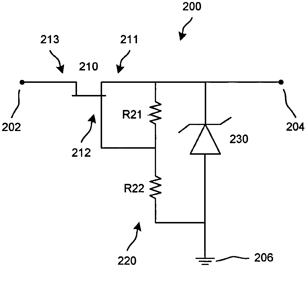
[0024] Input power protection device 100 is configured to provide power protection to load 140 from one or more undesirable power conditions. In some embodiments, undesired power conditions (which may include overvoltage conditions and/or overcurrent conditions) such as voltage spikes (related to power supply noise) and/or current spikes (caused by load switching) can be caused by power supply 150 yields. For example, load 140 may include electronic components that may be damaged in an undesired manner (eg, sensors, transistors, microprocessors, application-specific integrated circuits (ASICs), discrete components, circuit boards). Accordingly, input power protection device 100 may be configured to detect these relatively rapid increases in current and/or voltage and prevent them from damaging load 140 and/or other components (eg, circuit boards) associated with load 140 .
[0025] In some embodiments, overcurrent protection portion 110 and overvoltage protection portion 130 may be included in input power protection device 100 such that overcurrent protection portion 110 provides continuous overcurrent protection and overvoltage protection portion 130 provides shunt-to-ground overvoltage Protect. In some embodiments, the continuous overcurrent protection provided by the overcurrent protection section 110 and the shunt-to-ground overvoltage protection provided by the overvoltage protection section 130 may be integrated into a single package of the input power protection device 100 such that the input power protection Device 100 is a single discrete component.
[0026] The overvoltage protection portion 130 of the input power protection device 100 may be configured to protect the load 140 from, for example, a sudden or sustained increase in voltage generated by the power source 150 . In other words, the overvoltage protection portion 130 of the input power protection device 100 may be configured to provide voltage protection for the load 140 in response to, for example, an overvoltage event. In some embodiments, the overvoltage protection portion 130 of the input power protection device 100 may be configured to protect the load 140 from The voltage generated by the power supply 150 . In particular, the overvoltage protection portion 130 may be configured to limit (eg, clamp) the voltage across the overvoltage protection device (and downstream load) to a breakdown voltage (eg, threshold voltage, voltage limit, clamping voltage) place. When the overvoltage protection portion 130 is limiting the voltage at the breakdown voltage, the overvoltage protection portion 130 may be said to be in a breakdown state.
[0027] In some embodiments, the overvoltage protection portion 130 of the input power protection device 100 can be or include, for example, any type of depletion mode device and/or a transient voltage suppressor (TVS) (also referred to as transient voltage suppression device). In some embodiments, the overvoltage protection portion 130 of the input power protection device 100 can be or include, for example, any type of device configured to break down and limit (eg, clamp) voltage. The overvoltage protection portion 130 may include any type of device having a limiting voltage (eg, breakdown voltage) that varies with temperature and/or current. In particular, the overvoltage protection portion 130 may include any type of device having, for example, a limiting voltage with a positive temperature coefficient characteristic (eg, a limiting voltage that increases as temperature increases). In some embodiments, the overvoltage protection portion 130 of the input power protection device 100 may include one or more TVS diodes (eg, Zener diodes with positive temperature coefficients), one or more metal oxide varistors, and/or the like. Wait. For example, if the overvoltage protection portion 130 is or includes a TVS diode, the TVS diode may be configured to limit the voltage across the TVS diode to the TVS breakdown voltage.
[0028] Overcurrent protection portion 110 of input power protection device 100 may be configured to protect load 140 (and/or overvoltage protection portion 130 ) from sudden or sustained increases in current generated by, for example, power source 150 . In other words, the overcurrent protection portion 110 of the input power protection device 100 may be configured to provide current protection for the load 140 (and/or the overvoltage protection portion 130 ) in response to, for example, an overcurrent event. In some embodiments, the overcurrent protection portion 110 of the input power protection device 100 can be configured to based on one or more current conditions (eg, current level for a specified period of time, current exceeding a threshold voltage, short high current pulse) Instead, the load 140 (and/or the overvoltage protection portion 130 ) is protected from the current generated by the power source 150 .
[0029]In some embodiments, the overcurrent protection portion 110 can be or include a portion configured to cause the conduction state to change from the on state ( For example, a high conduction state, a low resistance state, a non-saturation state) changes to a current limiting state (e.g., a low conduction state, a high resistance state), which prevents or limits (significantly limits) the flow of current to the load 140 (and/or through overvoltage protection section 130). In some embodiments, the overcurrent protection portion 110 may saturate while in the current limiting state. When in a current limited state, current may be limited to a current limit, which may be referred to as saturation current limit or saturation current.
[0030] For example, in some embodiments, overcurrent protection portion 110 may be or may include any type of semiconductor device configured to limit current flow from power supply 150 to load 140 (and/or overvoltage protection portion 130 ). In some embodiments, the overcurrent protection portion 110 can be or include any type of saturation device configured to limit current (to current limit) based on an electric field. As a particular example, the overcurrent protection portion 110 may be or may include a junction field effect transistor (JFET) device, an accumulation channel field effect transistor (ACCUFET) device, and/or the like. If the overcurrent protection portion 110 includes a JFET device, the JFET device may be configured to limit the current through the JFET device to the saturation current of the JFET device when the JFET device saturates. Thus, in a current limiting state (which can occur when the JFET device is saturated), the JFET device can protect the load 140 (and/or the overvoltage protection section 130) from currents produced by the power supply 150 at (or above) the saturation current . In other words, when in the current limiting state, the JFET device can limit the current to the load 140 (and/or to the overvoltage protection portion 130 ) and produced by the power supply 150 to a saturation current. In some embodiments, after the overcurrent condition has ended, the overcurrent protection portion 110 may be configured to change the conduction state from a current limiting state (e.g., low conduction state, high resistance state) to an on state (e.g., high conductive state, low resistance state). In some embodiments, the JFET device may not saturate when in the on state.
[0031] In some embodiments, the current limiting capability of the overcurrent protection part 110 may vary when the overcurrent protection part 110 is in the current limiting state. For example, when the overcurrent protection part 110 is in the current limiting state, the current passing through the overcurrent protection part 110 can pass through the overcurrent The current of the protection part 110 is slightly reduced. The reduction of the current through the overcurrent protection portion 110 may be triggered by a voltage (also referred to as a control voltage) applied to the overcurrent protection portion 110 via, for example, a control pin. A change (eg, decrease, increase) in the voltage applied to the overcurrent protection portion 110 may trigger a further decrease in the current through the overcurrent protection portion 110 . In some embodiments, the overcurrent protection portion 110 may have a threshold control voltage that may decrease or increase the current through the overcurrent protection portion 110 .
[0032] As a specific example, if overcurrent protection portion 110 is a JFET device, then a specified gate voltage (e.g., a specified absolute value of the gate voltage, a specified negative gate voltage) applied to the JFET device (e.g., the gate pin of the JFET device) to source voltage (V GS )) can result in a reduction (eg, reduction) in the size of the channel (eg, conduction channel) of the JFET device and a corresponding decrease in current through the JFET device (due to the reduced saturation current of the JFET device). The size of the channel of the JFET device can be reduced (using the voltage applied to the gate of the JFET device) until current no longer flows (or substantially does not flow through) the JFET device. A JFET device is a class A semiconductor device configured to modulate the resistance of a channel within the JFET device in response to an applied voltage (eg, an applied negative voltage, an applied control voltage) on a gate of the JFET device.
[0033] In some embodiments, the overcurrent protection portion 110 of the input power protection device 100 may be or may include, for example, any type of device. In other words, the overcurrent protection portion 110 may include any type of current sensitive switching device having a current limiting state (eg, a high resistance state).
[0034] In some embodiments, the overcurrent protection portion 110 can be or include a portion configured to cause an open circuit (e.g., melt to create an open circuit, fuse to create an open circuit) that responds in response to an open circuit from the power supply 150 ( And prevents current from flowing to the load 140 when the current output through the overcurrent protection portion 110 exceeds the threshold current (within a specified period of time). For example, in some embodiments, the overcurrent protection portion 110 of the input power protection device 100 may be or include, for example, a fuse, a silicon current limit switch, a polysilicon based fuse, an electronic fuse (e fuse), polymer positive temperature coefficient (PPTC) devices, ceramic positive temperature coefficient (CPTC) devices, and/or the like. As a specific example, fuses may be used in conjunction with JFET devices within the overcurrent protection portion 110 .
[0035] In some embodiments, the overcurrent protection portion 110 and the overvoltage protection portion 130 can be configured to interoperate (eg, can be matched). In other words, overcurrent protection portion 110 and overvoltage protection portion 130 may be configured (eg, sized) such that overcurrent protection portion 110 and overvoltage protection portion 130 collectively operate in a desired manner. For example, the overvoltage protection portion 130 may be configured to cause the overcurrent protection portion 110 to change from an on state to a current limiting state.
[0036] In some embodiments, overvoltage protection portion 130 may be configured to cause overcurrent protection portion 110 to change to a current limiting state in response to overvoltage protection portion 130 being heated (eg, temperature increase, temperature increase in response to current flow). Heating of the overvoltage protection portion 130 may be caused by current passing through the overvoltage protection portion 130 (eg, current shunted through the overvoltage protection portion 130 ) and/or may be diverted from other components of the input power protection device 100 to the overvoltage protection portion 130 (eg, heat from the overcurrent protection portion 110 ) results. Accordingly, in some embodiments, the overvoltage protection portion 130 may be configured to cause the overcurrent protection portion 110 to change to a current limiting state in response to a current passing through the overvoltage protection portion 130 . As a specific example, a Zener diode included in the overvoltage protection part 130 may have a breakdown voltage that increases as temperature increases. An increase in the breakdown voltage of the zener diode within the overvoltage protection portion 130 may be used to trigger the overcurrent protection portion 110 to change to a current limiting state and limit the current through the overcurrent protection portion 110 .
[0037] In some embodiments, the overcurrent protection portion 110 can be or include a device that is biased to operate in an on state. In other words, the overcurrent protection portion 110 can operate in an on state until triggered to change to a current limiting state. In such embodiments, the overvoltage protection portion 130 may be configured to cause the overcurrent protection portion 110 to change from the on state to the current limiting state and remain in the current limiting state. Additionally, in such embodiments, the overcurrent protection portion 110 may change back from the current limiting state to the on state when the overvoltage protection portion 130 no longer triggers the overcurrent protection portion 110 to remain in the on state. For example, the overcurrent protection portion 110 may be or may include a JFET device that is biased (and configured) to operate in an on state (not limiting current during normal load 140 and/or power supply 150 operation), until the specified gate voltage (e.g., control voltage, specified negative gate-to-source voltage (V GS )) is applied to the JFET device to lower (eg, reduce, suppress) at least a portion of the conductive channel within the JFET device to the point where the JFET device limits current.
[0038] like figure 1 As shown in , the input power protection device 100 includes a control circuit 120 . Control circuit 120 may be configured to facilitate interaction between overvoltage protection portion 130 and overcurrent protection portion 110 . For example, the control circuit 120 may be configured to define a feedback signal (eg, a feedback voltage and/or a feedback current) that may be configured to trigger the overcurrent protection portion 110 to change the conduction state. The feedback signal may be defined (eg, generated) by the control circuit 120 based on the behavior of the overvoltage protection portion 130 . In some embodiments, the control circuit 120 may be any kind of control circuit configured to provide a feedback signal to the overcurrent protection portion 110 in response to a voltage across the overvoltage protection portion 130 (eg, a control voltage) such that the overcurrent protection portion 110 The current protection portion 110 operates in a current limiting state (eg, controls current, reduces current). In some embodiments, the control circuit 120 may include various types of devices, such as resistors, transistors, control circuits, and/or the like. For example, more details related to the interaction between the components of the input power protection device 100 are described in connection with the following figures.
[0039] In some embodiments, the interactions between components of the input power protection device 100 may be protective interactions. In other words, one component from the input power protection device 100 may be configured to protect another component of the input power protection device 100 . For example, the overcurrent protection portion 110 can be configured to change from an on state (non-saturated state) to a current limiting state such that the current through the overvoltage protection portion 130 can be limited by the overcurrent protection portion 110 . Additionally, the overvoltage protection portion 130 may be configured to limit voltage such that the voltage drop across the overcurrent protection portion 110 may also be limited. In some embodiments, the interaction of the overcurrent protection portion 110 (which reduces the power absorbed by the overvoltage protection portion 130 ) with the overvoltage protection portion 130 (which turns off the overcurrent protection portion 110 ) can cause the absorption ratio to be at no The input power protection components would have absorbed less power with the interaction between the overcurrent protection portion 110 and the overvoltage protection portion 130 as described herein. For example, more details related to mutual protection provided by components within input power protection device 100 are described in greater detail in connection with the following figures.
[0040] In some embodiments, the overcurrent protection part 110, the control circuit 120 and/or the overvoltage protection part 130 may be integrated into a single component. In other words, the overcurrent protection portion 110, the control circuit 120, and/or the overvoltage protection portion 130 may be integrated into the input power protection device 100 such that the input power protection device 100 is a single integrated component (eg, a single discrete component). In other words, the input power protection device 100 may be a single integrated component including the overcurrent protection part 110 , the control circuit 120 and/or the overvoltage protection part 130 . For example, the control circuit 120 and the overvoltage protection portion 130 may be integrated as a single discrete device, and the overcurrent protection portion 110 may be integrated as a separate single discrete device. In particular, the overcurrent protection portion 110, the control circuit 120, and/or the overvoltage protection portion 130 may be integrated into an input terminal having three terminals—an input terminal 102, an output terminal 104, and a ground terminal 106 (which may be collectively referred to as terminals). In a single package of the power protection device 100. In some embodiments, the terminals may be referred to as ports, pins, sections, and/or the like (eg, input port 102 may be referred to as input pin 102 or input section 102 ).
[0041]Since the overcurrent protection part 110 , the control circuit 120 and/or the overvoltage protection part 130 can be integrated into a single component, assembly can be simplified and production costs can be reduced. In some embodiments, the overcurrent protection portion 110, the control circuit 120, and/or the overvoltage protection portion 130 may be integrated into a single component (ie, the input power protection device 100), such that separate overcurrent protection devices and overvoltage protection devices Installation into a computing device (eg, such as computing device 10) may not be necessary. Instead, overcurrent protection and overvoltage protection may be provided by the input power protection device 100 , which includes both the overcurrent protection portion 110 and the overvoltage protection portion 130 . In some embodiments, circuit board space may be allocated more efficiently by using input power protection device 100 , which may be a single component, than if multiple separate components were used to implement overcurrent protection and overvoltage protection. In some embodiments, heat transfer between components of input power protection device 100 may be facilitated by integrating one or more of the components of input power protection device 100 into a single discrete component.
[0042] In summary, the voltage across the overvoltage protection portion 130 may be responsive to heat (which may be caused by the current passing through the overvoltage protection portion 130) and/or current (which may not cause heating of the overvoltage protection portion 130 if the current rises rapidly). ) increases and triggers the overcurrent protection part 110 to change to the current limiting state. The rise in voltage across overvoltage protection portion 130 in response to current flow (eg, only current flow) may be at least partially attributable to the resistance of overvoltage protection portion 130 . Furthermore, overcurrent protection portion 110 may change to (or may in) current limit state. Thus, combinations of scenarios, including any of the above, may trigger operation of the input power protection device 100 .
[0043] like figure 1 As shown in , input power protection device 100 , power supply 150 , and load 140 may be included in (eg, integrated into) computing device 10 . In some embodiments, computing device 10 may be, for example, a computer, a personal digital assistant (PDA), a host computer, a memory component (e.g., a hard disk drive), an adapter, an electronic measurement device, a data analysis device, a cellular phone, electronic devices and/or etc.
[0044] In some embodiments, power supply 150 may be any type of power supply such as, for example, a switched mode power supply, a direct current (DC) power supply, an alternating current (AC) power supply, and/or the like. In some embodiments, power source 150 may include a power source, which may be any type of power source, such as, for example, a direct current (DC) power source, such as a battery, a fuel unit, and/or the like.
[0045] In some embodiments, power supply 150 may be a signal source, such as a transmitter, configured to transmit one or more signals (eg, data signals). In some embodiments, the power source 150 may be coupled to the input power protection device 100 via wire or wirelessly. In such embodiments, one or more portions of input power protection device 100 may be included in a transceiver configured to receive one or more signals from power source 150 .
[0046] figure 2 is a schematic diagram of the components of the input power protection device 200 . like figure 2 As shown in , the input power protection device 200 includes a JFET device 210 that acts as the overcurrent protection portion of the input power protection device 200 . The input power protection device 200 also includes a Zener diode 230 (which may be a type of TVS diode and may be generally referred to as a Zener diode device), which acts as the overvoltage protection portion of the input power protection device 200 .
[0047] JFET device 210 may be configured to act as an electronically controlled switch or a voltage controlled resistor within input power protection device 200 . In some embodiments, JFET device 210 and/or Zener diode 230 can be made using any type of semiconductor material such as, for example, silicon (eg, doped silicon), gallium arsenide, germanium, silicon carbide, and A semiconductor device formed by a PN junction (which is formed with or associated with a p-type semiconductor and an n-type semiconductor) in /or etc.). In other words, JFET device 210 and/or Zener diode 230 may include a silicon substrate that includes (or is associated with) at least a portion of a PN junction. In some embodiments, a PN junction can be created in a single crystal or multiple crystals of a semiconductor, for example, by doping using ion implantation, diffusion of dopants, epitaxial growth, and/or the like.
[0048] like figure 2 As shown in , the input power protection device 200 includes a control circuit 220 . Specifically, in this embodiment, the control circuit 220 is a voltage divider including a resistor R21 and a resistor R22. Resistor R21 is coupled between gate 212 and source 211 of JFET 210 . Resistor R22 is coupled between gate 212 of JFET 210 and ground terminal 206 (also referred to as a ground node).
[0049] In this embodiment, the input power protection device 200 includes three terminals—an input terminal 202 , an output terminal 204 and a ground terminal 206 . like figure 2 As shown in , input terminal 202 is coupled (eg, electrically coupled) to drain 213 of JFET device 210 . Zener diode 230 is coupled (eg, electrically coupled) to source 211 of JFET device 210 , which is also coupled (eg, electrically coupled to) output terminal 204 . Thus, source 211 and Zener diode 230 of JFET device 210 are both coupled to output terminal 204 and act as a single node. Zener diode 230 is also coupled to ground terminal 206 .
[0050] In this embodiment, Zener diode 230 may have a breakdown voltage that increases with increasing temperature (ie, has a positive voltage coefficient) during, for example, an overvoltage event. An increase in the breakdown voltage of Zener diode 230 may be utilized via control circuit 220 to trigger JFET device 210 to change from the on state (the state to which JFET device 210 is biased) to the current limited state.
[0051] In particular, during an overvoltage event, Zener diode 230 may be configured to limit (eg, clamp) the voltage across the input power protection device (eg, across Zener diode 230 ) to the breakdown of Zener diode 230 Voltage. Zener diode 230 may shunt current associated with the overvoltage event to the ground node. Zener diode 230 (eg, the PN junction within Zener diode 230 ) may increase in temperature in response to current flowing through Zener diode 230 when current is shunted to the ground node. Therefore, the breakdown voltage of Zener diode 230 will increase in response to increasing temperature.
[0052] Resistors R21, R22 of the control circuit 220 may be configured to apply a voltage (e.g., a control voltage) to the JFET device 210 (e.g., to the gate 212 of the JFET device 210), which will cause it to be biased to an on-state The JFET device 210 changes from the on state to the current limiting state (which may occur when the JFET device 210 is saturated). In particular, resistors R21, R22 may be sized such that when the breakdown voltage of Zener diode 230 reaches a specified value, JFET device 210 will change (eg, begin to change) from an on state to a current limiting state (for a given current through the JFET device 210). In some embodiments, the breakdown voltage of Zener diode 230 at which JFET device 210 will change to a current limiting state may be referred to as a trigger breakdown voltage or a trigger breakdown point. In some embodiments, the voltage (eg, control voltage) applied to the gate 212 of the JFET device 210 may be referred to as a feedback voltage or a feedback signal. like figure 2 As shown in , the voltage across JFET device 210 (ie, the voltage across resistor R21 ) will be the voltage drop (ie, a negative voltage) from source 211 to gate 212 of JFET device 210 .
[0053] The breakdown voltage of the Zener diode 230 may increase as the temperature of the Zener diode 230 increases. The gate-to-source voltage of the JFET can be increased within the increasing voltage across the Zener diode 230 (which will be clamped at the breakdown voltage of the Zener diode 230) if the reference is an absolute voltage (or if the reference is a negative voltage is reduced). The resistance of JFET device 210 will increase with increasing gate voltage (eg, control voltage) and the current through JFET device 210 will decrease. The current through the JFET device 210 will decrease because the channel of the JFET device 210 will increase with the gate-to-source voltage (i.e., the absolute value of the gate-to-source voltage) when the JFET device 210 is in the current-limited state. and closed (eg, continue to close, gradually close, shut down, become restricted).
[0054] Figures 3A to 3C is a graph illustrating the operation of the input power protection device 200 . Specifically, Figure 3A is a graphic description figure 2 The graph of the breakdown voltage 30 of the Zener diode shown in . Figure 3B is a diagram that spans figure 2 The resistor voltage shown in V R21 and V R22 of the graph. Figure 3C is a diagram that passes through figure 2 The graph of current 35 for the JFET device shown in . like Figures 3A to 3C As shown in , the x-axis of each of the graphs is the temperature of the Zener diode and the temperature of the Zener diode is increasing to the right. Each of the graphs starts at the temperature T1 of the Zener diode and assumes that the Zener diode is in a breakdown state in response to an energy pulse (eg, an overvoltage event and/or an overcurrent event).
[0055] like Figure 3A As shown in , as the temperature of the Zener diode increases, the breakdown voltage 30 of the Zener diode increases. In this embodiment, the breakdown voltage 30 of the Zener diode increases in an approximately linear fashion. In some embodiments, the breakdown voltage 30 of the Zener diode may not increase in an approximately linear fashion. In some embodiments, the breakdown voltage 30 of the Zener diode may increase in response to current being shunted through the Zener diode (when the Zener diode is in a breakdown state). In some embodiments, the current shunted through the Zener diode may be associated with an energy pulse.
[0056] In some embodiments, temperature T1 may be about 0° C. and temperature T2 may be a temperature greater than T1 . In some embodiments, temperature T1 may be greater than 0°C (eg, 25°C) or less than 0°C (eg, -25°C). In some embodiments, temperature T2 may be 50°C or higher (eg, 100°C, 200°C, 300°C, 800°C). In some embodiments, the breakdown voltage can be, for example, between millivolts and volts. For example, the breakdown voltage can be 5 volts, 50 volts, and so on.
[0057] exist Figure 3B , the voltages V corresponding to resistors R21 and R22, respectively, are depicted with respect to ground R21 and V R22. Therefore, the voltage V R21 Following the breakdown voltage of the Zener diode 30, the voltage across resistor R21 is the voltage V R21 with voltage V R22 difference between. like Figure 3B As shown in , when the breakdown voltage 30 of the Zener diode increases with the temperature of the Zener diode, the voltage V R21 and V R22 also increase. In this embodiment, the gate-to-source voltage of the JFET device (which is negative) (i.e., the absolute value of the gate-to-source voltage) is the voltage across resistor R21, which is the voltage V R21 with voltage V R22 difference between.
[0058] like Figure 3CAs shown in , the current 37 through the JFET device is the saturation current 37 of the JFET device. Current 37 is shown as a dashed line because current 37 represents the theoretical maximum current through the JFET device when the JFET device is saturated. The saturation current 37 of the JFET device is a function of the gate-to-source voltage of the JFET device. like Figure 3C As shown in , the saturation current 37 increases with the gate-to-source voltage of the JFET device (which is shown in Figure 3B middle) because the channel of the JFET device decreases (or the resistance across the JFET device increases) as the gate-to-source voltage increases.
[0059] In addition, if Figure 3C As shown in , in this illustrative example, it is assumed that the current 35 through the JFET device is constant (or substantially constant) (and is operating (at least initially) just below the current 37 ) until the temperature of the Zener diode is at temperature T2. At temperature T2, the current 35 through the JFET device (which is the actual current obtained via the JFET device) intersects the current 37 through the JFET device when the JFET device is saturated.
[0060] When the temperature of the Zener diode reaches the temperature T2, the breakdown voltage 30 of the Zener diode is at the trigger breakdown voltage VTR, as Figure 3A shown in . When the trigger breakdown voltage VTR is reached at temperature T2, the gate-to-source voltage of the JFET device is Q, which is the voltage V R21 with voltage V R22 difference between Figure 3B shown in . When the gate-to-source voltage of the JFET device is Q, the JFET device changes from the on-state to the current-limited state, as Figure 3C shown in . like Figure 3C As shown in , the current 35 through the JFET device does not start to decrease and is not considered to be in a current limited state until the JFET device saturates. When in the current limited state, the current 35 through the JFET device decreases along a saturation current 37 curve.
[0061] When the breakdown voltage 30 of the Zener diode continues to increase as the temperature of the Zener diode increases beyond temperature T2 (shown in Figure 3A ), the gate-to-source voltage of the JFET device (V GS ) continues to increase (or decrease if the reference is a negative voltage) in absolute value (as Figure 3B shown in ). Consequently, the resistance of the JFET device increases and the current 30 through the JFET device decreases, as Figure 3C shown in . The current 30 through the JFET device decreases because the channel through the JFET device closes as the gate-to-source voltage (i.e., the absolute value of the gate-to-source voltage) increases when the JFET device is in a current-limited state (e.g. continue to close, shut down, limit).
[0062] In this embodiment, current 35 through the JFET device is constant (eg, substantially constant) between temperatures T1 and T2. In some embodiments, the current through the JFET device can vary (eg, increase, decrease) based on the energy pulse coupled to the input power protection device and/or the characteristics of the component.
[0063] Although not shown, if the current 35 through the JFET device is higher than Figure 3C The current shown in , then the temperature of the Zener diode where the current 35 through the JFET device will be limited will be lower than the temperature T2. Therefore, the JFET device will change from the on state to the current limiting state at a temperature lower than the temperature T2. Furthermore, due to the higher current 35 (which will also flow through the Zener diode), the temperature of the Zener diode is comparable to Figure 3A Associations increase more rapidly (eg, during shorter time periods). Thus, Zener diode and JFET devices can provide faster power protection for relatively high energy pulses (eg, relatively high current) than for relatively low energy pulses (eg, relatively low current).
[0064] back reference figure 2 , JFET device 210 is configured to float above ground via resistor R22. Thus, JFET device 210 does not need to be configured to handle the full rail-to-ground voltage, which is handled by Zener diode 230 . Thus, in some embodiments, JFET device 210 may be configured with a lower voltage rating than would be required if tied to ground. Furthermore, since the current through the Zener diode 230 will limit the saturation current to the JFET device 210 (and since the Zener diode 230 thermally triggers the JFET device 210 to reduce its current in response to the temperature rise of the Zener diode 230), the Zener diode 230 is sized (eg, sized down) according to the saturation current of JFET device 210 .
[0065] Furthermore, as the resistance of JFET device 210 increases, the current through JFET device 210 will decrease and result in a lower current through Zener diode 230 . In some examples, this lower current through Zener diode 230 will result in a lower temperature of Zener diode 230 (if the current is reduced for a sufficient period of time) and a lower voltage across Zener diode 230 . This lower voltage across Zener diode 230 will counteract the increase in resistance of JFET device 210 . These opposing forces may result in steady state operation of the input power protection device 200 . When the input power protection device 200 is operating in steady state, the heating rate of the Zener diode 230 will be in steady state (when the current through the Zener diode 230 is fixed). In some embodiments, these opposing forces may cause oscillations in the operation of the input power protection device 200 until a steady state operating point for the input power device 200 is reached. combine Figures 5A to 5E Steady state operation of input power devices is discussed in more detail.
[0066] Although this embodiment, and many of the embodiments described herein, are discussed in the context of Zener diodes and JFET devices, many types of overvoltage protection sections and/or overcurrent protection sections can be combined with Zener diodes and/or JFET devices are used with or in place of Zener diodes and/or JFET devices. For example, the overvoltage protection portion of the input power protection device 200 may be any type of device that has a breakdown voltage that changes (eg, increases with temperature) with temperature. The overcurrent protection portion of input power protection device 200 may be any type of device that can be biased to an on state while in a current limiting state, change from an on state to a current limiting state, and limit the current flow through the device .
[0067] Figures 4A to 4E is a graph illustrating the behavior of the components of an input power protection device in response to a pulse of energy. Input power protection devices include overvoltage protection devices, control circuits and overcurrent protection devices, such as figure 1 and 2 those shown in . The graphs illustrate power protection provided by components of an input power protection device in response to energy pulses.
[0068] Figure 4A is a graph illustrating the voltage across an overvoltage protective device, Figure 4B is a graph illustrating the state of the overvoltage protection device, and Figure 4C is a graph illustrating the temperature of an overvoltage protection device. Figure 4D is a graph illustrating the state of the overcurrent protection device, and Figure 4E is a graph illustrating the current flow through an overcurrent protection device. exist Figures 4A to 4E In , time is increasing to the right, and the energy pulse begins at approximately time U1 and ends at approximately time U2.
[0069] like Figure 4A As shown in , the voltage across the overvoltage protection device increases steeply at about time U1 in response to the energy pulse beginning at about time U1. In this embodiment, the overvoltage protection device, which may be a Zener diode, changes from a non-breakdown state (e.g., normal operating state, off state) to a breakdown state between approximately times U1 and U2 in response to the energy pulse. wear state, such as Figure 4B shown in . Thus, the voltage across the overvoltage protection device between times U1 and U2 (during the time period between times U1 and U2 ) is approximately the breakdown voltage of the overvoltage protection device.
[0070] Furthermore, in response to the energy pulse, the temperature of the overvoltage protection device (e.g., the temperature of the junction of the semiconductor substrate of the overvoltage protection device, the temperature of the semiconductor substrate of the overvoltage protection device) begins to increase at about time U1, as Figure 4C shown in . In this embodiment, the temperature of the overvoltage protection device increases approximately linearly.
[0071] like Figure 4A as shown in , in response to the Figure 4C As the temperature of the overvoltage protection device in increases, the voltage across the overvoltage protection device increases approximately linearly between times U1 and U2. In other words, the breakdown voltage of the overvoltage protection device increases in response to increasing temperature. Consequently, the voltage across the overvoltage protection device, which is clamped at the breakdown voltage, also increases.
[0072] like Figure 4A As shown in , the voltage across the voltage protection device does not rise to trigger the breakdown voltage VTX. Although not shown, in some embodiments, when the Zener diode is in a breakdown state, the voltage across the Zener diode may increase between times U1 and U2 in response to current being shunted through the Zener diode. The current shunted through the Zener diode can be associated with an energy pulse. Although not shown, in some embodiments, if the duration of the energy pulse is longer than the time period between times U1 and U2 (eg Figure 4A ), then the voltage across the overvoltage protection device has increased beyond the breakdown voltage VTX.
[0073] as well Figure 4C As shown in , the temperature of the overvoltage protection device remains below the failure temperature FT (also referred to as the breakdown temperature). In some embodiments, the overvoltage protection device may fail when the temperature of the overvoltage protection device exceeds the failure temperature FT. For example, if the overvoltage protection device is a Zener diode, metal migration across the PN junction of the Zener diode in response to a temperature above the failure temperature FT of the Zener diode can result in junction) short circuit.
[0074] In some embodiments, the rate of temperature increase of the overvoltage protection device may depend on, for example, the packaging (or lack thereof) surrounding the overvoltage protection device, heat (or lack thereof) from other devices surrounding the overvoltage protection device ) and/or etc. For example, in some embodiments, one or more heat sinks (e.g., semiconductor components, packages) associated with (e.g., coupled to, around) the overvoltage protection device may be configured such that they absorb Heat that would otherwise be directed to the overvoltage protection device. In such instances, the rate of temperature increase of the overvoltage protection device in response to the energy pulse may be faster than without the heat sink. In some embodiments, an overvoltage protection device may be associated with one or more heat sources (e.g., devices, resistors) (and/or insulators) configured to direct (and/or contain) nano) heat to the overvoltage protection device such that the temperature of the overvoltage protection device increases and the resulting voltage across the overvoltage protection device (while in a breakdown state) will increase at a relatively rapid rate (e.g., within a threshold time period exceeds the trigger breakdown voltage VTX).
[0075] like Figure 4D As shown in , the overcurrent protection device remains in a non-saturated on state because the feedback signal from the control circuit does not cause the overcurrent protection device to change to the current limiting state in response to the voltage across the overvoltage protection device. In this embodiment, the control circuit is configured to cause the overcurrent protection device to change to the on state in response to the voltage across the overvoltage protection device rising to the trigger breakdown voltage VTX.
[0076]Although not shown, the overcurrent protection device may change from the on state to the current limiting state if the voltage across the overvoltage protection device has risen to or above the trigger breakdown voltage VTX. The change may be triggered by the control circuit in response to the voltage across the overvoltage protection device rising to or exceeding the trigger breakdown voltage VTX. In such examples, the current through the overcurrent protection device and/or the overvoltage protection device may be limited (eg, reduced) when the overcurrent protection device is in a current limiting state.
[0077] like Figure 4E As shown in , the current through the overcurrent protection device increases at approximately time U1 and remains at an increasing level during the energy pulse between times U1 and U2. like Figure 4E As shown in , the current associated with the energy pulse is substantially constant in this embodiment. Although not shown, in some embodiments, the current (and/or voltage) associated with the energy pulse can vary. In these examples, the current through the overcurrent protection device can vary, the temperature of the overvoltage protection device (shown in Figure 4A middle) can increase in a non-linear fashion and/or the voltage across the overvoltage protection device (shown in Figure 4C Middle) can also be increased in a non-linear fashion.
[0078] Although the saturation current is not shown, the current through the overcurrent protection device does not reach the saturation current of the overcurrent protection device. Therefore, the overcurrent protection device does not change to the current limiting state. In some embodiments, when an overcurrent protection device (eg, a JFET, for example) saturates, the current associated with the energy pulse may be limited to a saturation current. Additionally, although not shown, the temperature of the overcurrent protection device is also kept below the failure temperature of the overcurrent protection device.
[0079] Figures 5A to 5E is a graph illustrating the behavior of components of an input power protection device in response to another pulse of energy. Input power protection devices include overvoltage protection devices, control circuits and overcurrent protection devices, such as figure 1 and 2 those shown in . The graphs illustrate power protection provided by components of an input power protection device in response to energy pulses.
[0080] Specifically, Figure 5A is a graph illustrating the voltage across an overvoltage protective device, Figure 5B is a graph illustrating the current flow through the overvoltage protection device, and Figure 5C is a graph illustrating the temperature of an overvoltage protection device. Figure 5D is a graph illustrating the current flow through the overcurrent protection device, and Figure 5E is a graph illustrating the voltage across an overcurrent protection device. exist Figures 5A to 5E , time is increasing to the right, and the energy pulse begins approximately at time S1 and continues beyond (eg, continues beyond) time S3.
[0081] like Figure 5A As shown in , the voltage across the overvoltage protection device increases steeply at about time S1 in response to the energy pulse beginning at about time S1. In this embodiment, the overvoltage protection device, which may be a Zener diode, changes from a non-breakdown state (eg, normal operating state, off state) to a breakdown state at approximately time S1 in response to the energy pulse. Therefore, the voltage across the overvoltage protection device beyond time S1 is approximately the breakdown voltage of the overvoltage protection device.
[0082] like Figure 5B As shown in , the current from the energy pulse begins to flow through the overvoltage protection device in response to the overvoltage protection device changing from a non-breakdown state (e.g., normal operating state, off state) to a breakdown state at approximately time S1 . In other words, when the overvoltage protection device changes to the breakdown state in response to the energy pulse, the overvoltage protection device begins to shunt current associated with the energy pulse through the overvoltage protection device. The shunting of current through the overvoltage protection device results in an increase in the temperature of the overvoltage protection device (starting at approximately time S1 as Figure 5C shown in ).
[0083] The temperature of the overvoltage protection device (e.g., the temperature of the junction of the semiconductor substrate of the overvoltage protection device, the temperature of the semiconductor substrate of the overvoltage protection device) begins to increase at about time S1 until shortly after time S2, as Figure 5C shown in . In this embodiment, the temperature of the overvoltage protection device increases approximately linearly between times S1 and S2. as combined Figures 4A to 4E As described, the rate at which the temperature of the overvoltage protection device increases may depend on the heat sink, heat source, and/or the like.
[0084] like Figure 5A As shown in , when in the breakdown state, the voltage across the overvoltage protection device increases as the temperature of the overvoltage protection device increases, as Figure 5C shown in . In this embodiment, the voltage across the overvoltage protection device, which is approximately equal to the breakdown voltage of the overvoltage protection device, reaches or exceeds the trigger breakdown voltage VTX at approximately time S2.
[0085] as well Figure 5C As shown in , the temperature of the overvoltage protection device remains below the failure temperature FT (also referred to as the breakdown temperature). In some embodiments, the overvoltage protection device may fail when the temperature of the overvoltage protection device exceeds the failure temperature FT. For example, if the overvoltage protection device is a Zener diode, metal migration across the PN junction of the Zener diode in response to a temperature above the failure temperature FT of the Zener diode can result in junction) short circuit.
[0086] like Figure 5D As shown in , the current through the overcurrent protection device increases at approximately time S1 and remains at an increasing level between times S1 and S2. like Figure 5D As shown in , the current associated with the energy pulse is substantially constant in this embodiment. Although not shown, in some embodiments, the current (and/or voltage) associated with the energy pulse can vary. In these examples, the current through the overcurrent protection device can vary, the temperature of the overvoltage protection device (shown in Figure 5A middle) can increase in a non-linear fashion and/or the voltage across the overvoltage protection device (shown in Figure 5B Middle) can also be increased in a non-linear fashion.
[0087] Although the saturation current is not shown, the current through the overcurrent protection device did not reach the saturation current of the overcurrent protection device between times S1 and S2. Additionally, although not shown, the temperature of the overcurrent protection device is also kept below the failure temperature of the overcurrent protection device.
[0088] like Figure 5D As shown in , the overcurrent protection device changes from the on state (while in the non-saturated state) to the current limiting state at approximately time S2. In this embodiment, the overcurrent protection device changes to the current limiting state in response to the voltage across the overvoltage protection device rising to the trigger breakdown voltage VTX. In some embodiments, the overcurrent protection device may be triggered to change from the on state to the current limiting state at approximately time S2 via a control circuit based on the voltage of the overvoltage protection device reaching or exceeding the trigger breakdown voltage VTX to generate a feedback signal.
[0089] When in the current limiting state (approximately after time S2), the overcurrent protection device saturates. Therefore, the current through the overcurrent protection device is limited by the saturation of the overcurrent protection device. like Figure 5D As shown in , the current through the overcurrent protection device begins to decrease at about time S2 until about time S3.
[0090] like Figure 5E As shown in , the voltage across the overcurrent protection device initially increases (from nominal or zero voltage) at approximately time S1 as the energy pulse begins. The reduced current through the overcurrent protection device corresponds to an additional increase in voltage across the overcurrent protection device (starting at approximately time S2) (as Figure 5E ), which results in a reduced saturation current of the overcurrent protection device. In other words, the voltage drop across the overcurrent protection device increases and causes the overcurrent protection device to limit current (while in the current limiting state) (limiting to the saturation current of the overcurrent protection device).
[0091] Responsive to the overcurrent protection device reducing the current when it is in the current limit state (as Figure 5D As shown in ), the current through the overvoltage protection device also starts to decrease at about time S2, as Figure 5B shown in . The reduced current through the overvoltage protection device results in a reduction in the rate of temperature increase of the overvoltage protection device, as Figure 5C shown in .
[0092] Although not shown, in some embodiments, a time delay in the temperature reduction of the overvoltage protection device (and/or other components of the input power protection device) may occur during operation of the input power protection device. In some embodiments, the time delay may be caused by heat stored in components surrounding the overvoltage protection device and/or the overcurrent protection device to achieve a hysteresis effect. In some embodiments, the temperature of the overvoltage protection device may decrease immediately (substantially immediately) in response to current being limited by the overcurrent protection device (while in the current limiting state).
[0093] like Figure 5C As demonstrated in , a reduction in the temperature of the overvoltage protection device can result in Figure 5A The drop in voltage across the overvoltage protection device shown in . However, as the energy pulse continues beyond time S3, the overvoltage protection device remains in a breakdown state (and has a voltage approximately at the breakdown voltage).
[0094] In this embodiment, the input power protection device reaches a steady state operating point after the voltage across the overvoltage protection device exceeds the trigger breakdown voltage VTX. In this embodiment, the steady-state operating point of the device is asymptotically obtained around time S3, as Figures 5A to 5E shown in . The steady state operating point of the input power protection device is obtained through voltage, current and temperature interactions between components of the input power protection device. This steady state operation capability is superior to silicon switch-type devices that may not continue to operate during transient events (eg, energy pulse events).
[0095] Specifically, when the voltage across the overvoltage protection device increases with the current flow through the overvoltage protection device (shown in Figure 5B ) resulting in a temperature increase (shown in Figure 5C ) while increasing beyond the trigger breakdown voltage VTX (shown in Figure 5A ), the current through the overcurrent protection device (shown in Figure 5D middle) decrease. In a feedback manner, the overcurrent protection device reduces the current through the overcurrent protection device (shown in Figure 5D ), which also reduces the current flowing through the overvoltage protection device (shown in Figure 5B ), which results in a reduced temperature (shown in Figure 5C ) and the reduced voltage across the overvoltage protection device (shown in Figure 5A Medium) (which can remain above the trigger breakdown voltage VTX). Ultimately, the components of the input power protection device are fixed at steady state operating points based on these canceling interactions. In some embodiments, the input power protection device may oscillate before settling at a steady state operating point.
[0096] although Figures 5A to 5E Not shown in , but in some embodiments, oscillations may occur before a steady state operating point is obtained at approximately time S3. Although not explicitly shown, the voltage across the overvoltage protection device is a function of both current and temperature. Thus, higher current pulses can result in current limiting (eg, faster current limiting than shown) at lower temperatures (which can lead to improved power protection). In such embodiments, the power protection can be performed on such as Figures 5A to 5E Occurs (or can be triggered) earlier than time S2 illustrated in .
[0097] despite the combination Figures 3A to 5EThe behavior of the described components is described as transitioning, for example, at specified voltages, currents, and/or at specified times, but when implemented (eg, using semiconductor devices), the transitions of the components may be slightly Occurs before the specified voltage, current and/or specified time or occurs slightly after the specified voltage, current and/or specified time. In particular, variations in breakdown voltage, thermal conductivity, processing variations, temperature variations, switching times of devices, circuit transition delays, and/or the like can result in voltage, current, temperature, and Conditions (eg, non-ideal conditions) that trigger transitions of components before and/or times before or slightly after the voltages, currents, temperatures and/or times shown in 3A-5E.
[0098] Image 6 is a schematic diagram of an input power protection device 600 including a control circuit 620 . like Image 6 As shown in , the input power protection device 600 includes a JFET device 610 that acts as the overcurrent protection portion of the input power protection device 600 . The input power protection device 600 also includes a Zener diode 630 (which may be a type of TVS diode and may be generally referred to as a Zener diode device), which acts as the overvoltage protection portion of the input power protection device 600 .
[0099] Image 6 The control circuit 620 shown in can be any kind of control circuit configured to provide a feedback signal to the JFET device 610 in response to the voltage across the Zener diode 630 such that the JFET device 610 operates in a current limited state. In some embodiments, control circuitry 620 may be or include, for example, electronic components, sensors, transistors, microprocessors, application specific integrated circuits (ASICs), discrete components, and/or the like.
[0100] Figure 7 is a schematic diagram of another input power protection device 700 including a control circuit 720 . like Figure 7 As shown in , the input power protection device 700 includes a JFET device 710 that acts as the overcurrent protection portion of the input power protection device 700 . The input power protection device 700 also includes a Zener diode 730 (which may be a type of TVS diode and may be generally referred to as a Zener diode device), which acts as the overvoltage protection portion of the input power protection device 700 .
[0101] Figure 7 The control circuit 720 shown in includes a resistor 724 and a Zener diode 722 . Resistor 724 is coupled between gate 712 and source 711 of JFET device 710 . In this embodiment, Zener diode 722 is configured to cause JFET device 710 to change to a current-limiting state and completely (or nearly completely) turn off the channel of JFET device 710 in response to Zener diode 722 failing short circuit (so that no current flows. flow through the JFET device 710).
[0102] In particular, Zener diode 722 may be configured to change the conduction state from a voltage regulation state to a short circuit state (eg, a high conduction/low resistance state), which is a thermally induced short state (eg, a non-reversible short state). When in a voltage regulation state, Zener diode 722 may be configured to limit (e.g., clamp) the voltage at a breakdown voltage (e.g., voltage limit, clamp voltage), thereby increasing the resistance of JFET device 710 to Zener diode 730. Sensitivity to voltage changes. In some embodiments, the resistance of resistor 724 and/or the electrical capacity of Zener diode 722 can be configured (eg, using doping concentrations and/or metal structures) such that the shorted state of Zener diode 722 can be A failure mode of the device in which a physical change in the structure of the Zener diode 722 results in a short circuit. In particular, Zener diode 722 may be configured to change from a voltage regulation state to a short circuit state in response to a temperature of Zener diode 722 increasing beyond a threshold temperature (eg, failure temperature, short circuit temperature). For example, in response to a temperature above the threshold temperature BT of Zener diode 722 (generated by internal heating and/or heat from JFET device 710, resistor 724, and/or Zener diode 730) across Zener diode 722 Metal migration of the PN junction can cause a short within Zener diode 722 (eg, across the PN junction). In some embodiments, the threshold temperature BT may be between, for example, 200 and 700 degrees Fahrenheit (eg, 350 degrees Fahrenheit, 400 degrees Fahrenheit, 450 degrees Fahrenheit).
[0103] In some embodiments, once Zener diode 722 has changed to the short circuit state, Zener diode 722 cannot change back to the voltage regulation state. In other words, the change from the voltage regulated state to the shorted state may be an irreversible change (eg, a physical change). Figure 7 The non-reversible operation of the input power protection device 700 illustrated in , as opposed to the reversible operation of the input power protection device described above.
[0104] In some embodiments, the operation of Zener diode 722 may be separated from the short state operation of Zener diode 730 . In other words, Zener diode 730 may be configured to trigger JFET device 710 to change to a current limiting state without Zener diode 722 failing short. Likewise, Zener diode 722 can be configured to change to a short circuit state and can cause JFET device 710 to change to a current limiting state (and off). In some embodiments, Zener diode 722 may be configured to change to a reversible thermal short (or highly conductive) state due to a thermally induced second breakdown mechanism. The temperature of the reversible thermal short state can be defined using, for example, the doping concentration within Zener diode 722 .
[0105] Figure 8A is a schematic diagram of yet another input power protection device 800 including a control circuit 820 . like Figure 8A As shown in , the input power protection device 800 includes a JFET device 810 that acts as the overcurrent protection portion of the input power protection device 800 . The input power protection device 800 also includes a Zener diode 830 (which may be a type of TVS diode and may be generally referred to as a Zener diode device), which acts as the overvoltage protection portion of the input power protection device 800 .
[0106] Figure 8A The control circuit 820 shown in includes a resistor 824 and a forward biased diode 822 (which includes diodes D1 through DN). Resistor 824 is coupled between gate 812 and source 811 of JFET device 810 . In this embodiment, diode 822 is configured to operate with Zener diode 830 to speed up the change of JFET device 810 to a current-limited state. In particular, diode 822 may be configured to pull the voltage of gate 812 of JFET device 810 toward ground in response to an increase in temperature of diode 822 . In some embodiments, diodes 822 may include more than 3 diodes (eg, 25 diodes, 100 diodes). In some embodiments, diodes 822 may include 3 or fewer diodes (eg, one diode, two diodes).
[0107] like Figure 8A As shown in , the temperature of diode 822 may increase in response to heat H1 transferred from JFET device 810 to diode 822 . Additionally, the temperature of diode 822 may increase in response to heat H2 transferred from Zener diode 830 to diode 822 . In some embodiments, heat H2 may be generated in response to current flowing through Zener diode 830 . In some embodiments, the temperature of diode 822 may increase in response to current flowing through diode 822 , which may be forward biased when current is flowing through diode 822 .
[0108] In some embodiments, resistor 724 (which may be thermally coupled to JFET device 810 and/or Zener diode 830 ) may have a positive temperature coefficient (PTC) to facilitate (or primarily cause) an accelerated turn-off of JFET device 810 . In some embodiments, a resistor with a negative temperature coefficient (NTC), which may be thermally coupled to JFET device 810 and/or Zener diode 830, may be used in place of one or more of diodes 822 to generate Diode 822 produces an accelerated turn-off effect. In some embodiments, the use of one or more NTC and/or PTC resistor devices eliminates the need for Zener diode 830 to exhibit PTC characteristics.
[0109] Figure 8B is a schematic illustration of Zener diode 830 and Figure 8A The graph of the temperature characteristic of diode 822 shown in . Figure 8B The graph in assumes that diodes 822 consist of 24 diodes (with a room temperature forward voltage drop of approximately 0.7V). like Figure 8B As shown in , the voltage 82 across the diode 822 decreases with increasing temperature, and the voltage 84 across the Zener diode increases with increasing temperature. The voltage 84 across the Zener diode 830 is about 13.2V at greater than 25°C, and the voltage 82 across the diode 822 is about 16.6V at about 25°C.
[0110] like Figure 8B As shown in , the gate-to-source voltage (V GS ) is approximately 0V because it is the point at which the voltage across diode 822 equals the voltage across Zener diode 830 (assuming input power protection device 800 is receiving energy pulses and resistance 824 is relatively small). At temperatures in excess of 160° C., the difference between the voltage 84 across the Zener diode 830 and the voltage 82 across the diode 822 can drive an increase in the gate voltage applied to the JFET device 810 . In some embodiments, even the channel of JFET device 810 may begin to turn off at temperatures greater than about 160°C. JFET device 810 may not limit the current through JFET device 810 because JFET device 810 may not yet be saturated. like Figure 8B As shown in , the positive temperature coefficient of the breakdown voltage of Zener diode 830 is used in conjunction with the negative temperature coefficient of diode 822 to trigger JFET device 810 to limit the current through JFET device 810 .
[0111] Figure 8C is a graphic description Figure 8A A table of example specifications for the components of the input power protection device 800 shown in . In this embodiment, when the VGS of Zener diode 830 is exceeded, JFET device 810 will be completely off (or nearly completely off). Although not shown, the JFET can be reduced by increasing the breakdown voltage of Zener diode 830 and/or by reducing the overall voltage drop across diodes 822 (either through fewer diodes or reducing the forward drop voltage of at least some of diodes 822). The temperature at which device 810 turns off (or nearly turns off completely). . It follows that the JFET device can be increased by reducing the breakdown voltage of the Zener diode 830 and/or by increasing the total voltage drop of the diodes 822 (either through more diodes or increasing the forward drop voltage of at least some of the diodes 822). The temperature at which the 810 turns off (or nearly turns off). Similarly, the JFET devices 810 can be configured to saturate and respectively at the V of the JFET devices 810 GS Turn off (or almost completely turn off) at a lower or higher voltage with a decrease or increase in the turn-off voltage.
[0112] presented by way of example only Figure 8C parameters shown in . In some embodiments, the parameters of JFET device 810 may be different from Figure 8C parameters shown in . For example, the minimum BV GDS Can be higher than 26V or lower than 26V. As another example, V G (shutdown) can be above -2V or below -2V.
[0113] Figure 9 is a flowchart illustrating a method for operating an input power protection device. The input power protection device can be combined with the input power protection device described above (for example, figure 1 One or more of the described input power protection devices 100) are similar or identical.
[0114] like Figure 9 As shown in , current is received at the overvoltage protection device while the overvoltage protection device is in a breakdown state (block 910). In some embodiments, the current may be associated with a transient event (eg, a pulse of energy). In some embodiments, a transient event may be configured to trigger the overvoltage protection device to change to a breakdown state. In some embodiments, the overvoltage protection device may be a Zener diode.
[0115] A feedback voltage is generated based on the current and based on a breakdown voltage of the overvoltage protection device (block 920). In some embodiments, the feedback voltage is a function of the voltage rise of the overvoltage protection device based on temperature as a function of the current through the overvoltage protection device. In some embodiments, the feedback voltage may be generated by a control circuit. In some embodiments, the control circuit may include one or more resistors, diodes, Zener diodes, and/or the like. In some embodiments, the control circuit may include one or more components having a voltage that decreases in response to temperature. Accordingly, at least one or more portions of the control circuit may have a negative temperature coefficient.
[0116] The feedback voltage is provided to an overcurrent protection device coupled to the overvoltage protection device (block 930). In some embodiments, the overcurrent protection device may be a JFET device, an ACCUFET device, and/or the like. In some embodiments, the overcurrent protection device may be disposed in series within the input power protection device and may have an output terminal coupled to the overvoltage protection device. In some embodiments, the feedback voltage may be provided by a control circuit coupled to the overcurrent protection device and the overvoltage protection device.
[0117] Changing the overcurrent protection device from an on state to a current limiting state or reducing the current limit of the current limiting state in response to temperature (block 940). In some embodiments, the overcurrent protection device may be configured to operate in saturation when in a current limiting state. In some embodiments, the breakdown voltage of the overvoltage protection device may increase in response to heat. Accordingly, the overvoltage protection device may have a breakdown voltage with a positive temperature coefficient. In some embodiments, the point at which the overcurrent protection device changes to the current limiting state may depend on the level of energy (eg, level of current, level of heat) associated with the energy pulse. In some embodiments, one or more portions of the input power protection device may be integrated into a single discrete component to facilitate heat transfer between portions of the input power protection device.
[0118] In one general aspect, an apparatus may include an overcurrent protection device and an overvoltage protection device coupled to the overcurrent protection device and configured to operate at a breakdown voltage of the overvoltage protection device The increase in response to heat then causes the overcurrent protection device to reduce current through the overvoltage protection device.
[0119] Embodiments of the various techniques described herein may be implemented in digital electronic circuitry or in computer hardware, firmware, software, or combinations thereof. Portions of the methods can be performed by, and devices (e.g., input power protection devices) can be implemented in special purpose logic circuits (e.g., FPGAs (Field Programmable Gate Arrays or ASICs (Application Specific Integrated Circuits)) Field Programmable Gate Array or ASIC (Application Specific Integrated Circuit)).
[0120] Some implementations may be implemented using various semiconductor processing and/or packaging techniques. Some embodiments may use various types of semiconductors associated with semiconductor substrates including, but not limited to, for example, silicon (Si), gallium arsenide (GaAs), silicon carbide (SiC), and/or the like. processing technology.
[0121] While certain features of the described implementations have been illustrated as described herein, many modifications, substitutions, changes and equivalents will now occur to those skilled in the art. It is, therefore, to be understood that the appended claims are intended to cover all such modifications and changes as fall within the scope of the described embodiments. It should be understood that the described embodiments have been presented by way of example only, not limitation, and that various changes in form and detail may be made. Any portion of the apparatus and/or methods described herein may be combined in any combination, except mutually exclusive combinations. The embodiments described herein can include various combinations and/or sub-combinations of the functions, components and/or features of the different described embodiments.
PUM


Description & Claims & Application Information
We can also present the details of the Description, Claims and Application information to help users get a comprehensive understanding of the technical details of the patent, such as background art, summary of invention, brief description of drawings, description of embodiments, and other original content. On the other hand, users can also determine the specific scope of protection of the technology through the list of claims; as well as understand the changes in the life cycle of the technology with the presentation of the patent timeline. Login to view more.