
Manufacture method of all-dielectric isolation silicon on insulator (SOI) material sheet for complementary bipolar process
A bipolar process and manufacturing method technology, applied in semiconductor/solid-state device manufacturing, electrical components, circuits, etc., can solve problems such as pattern drift, poor consistency of active layer parameters, and achieve good consistency, low production cost, and omission of Effects of Epitaxy Process
- Summary
- Abstract
- Description
- Claims
- Application Information
AI Technical Summary
Problems solved by technology
Method used
Image

Examples
Embodiment Construction
[0036] The method of the present invention will be further described below in conjunction with the accompanying drawings and embodiments. The technical solution of the present invention is not limited to the description of this embodiment.
[0037] The specific manufacturing steps of this embodiment are as follows:
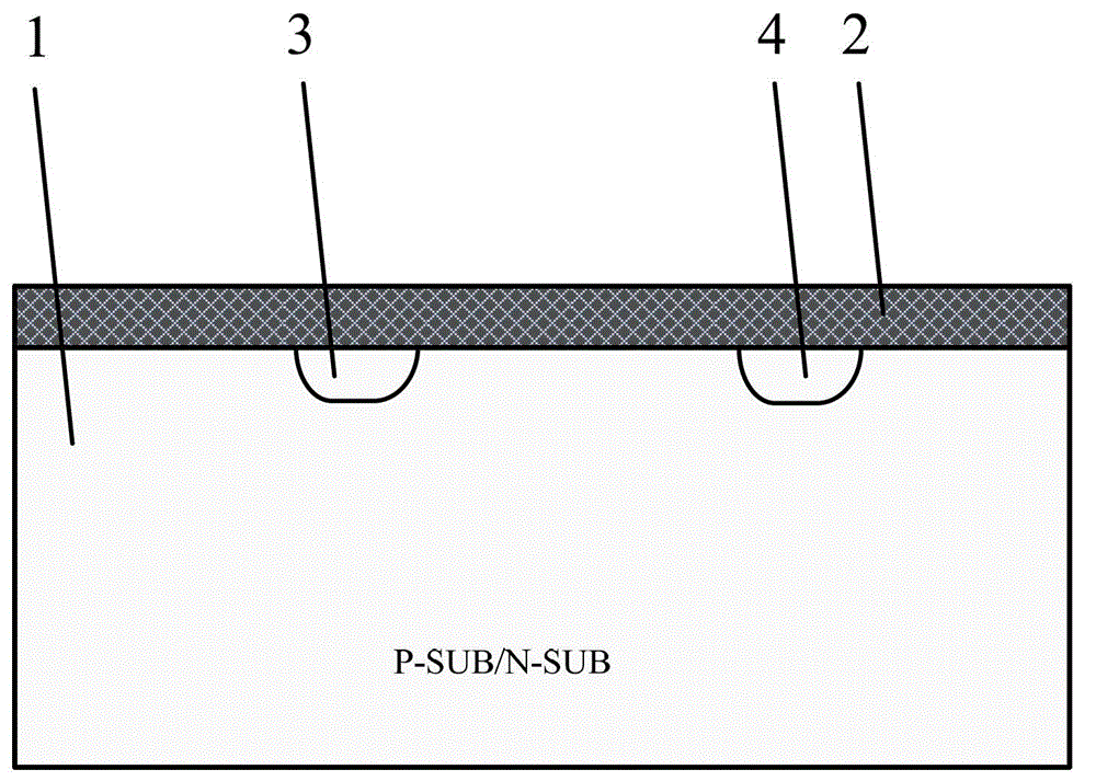
[0038] (1) Make N-type buried layer 3 and P-type buried layer 4 on monocrystalline silicon wafer one:
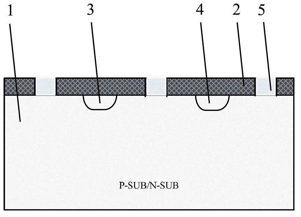
[0039] Form a zero-layer mark on the single crystal silicon wafer 1, grow a thin oxide layer 2 with a thickness of 13.5-15.5nm at 950°C, and make an N-type buried layer 3 and a P-type buried layer 4, and anneal at 1050°C for 55 minutes ,Such as figure 1 shown.
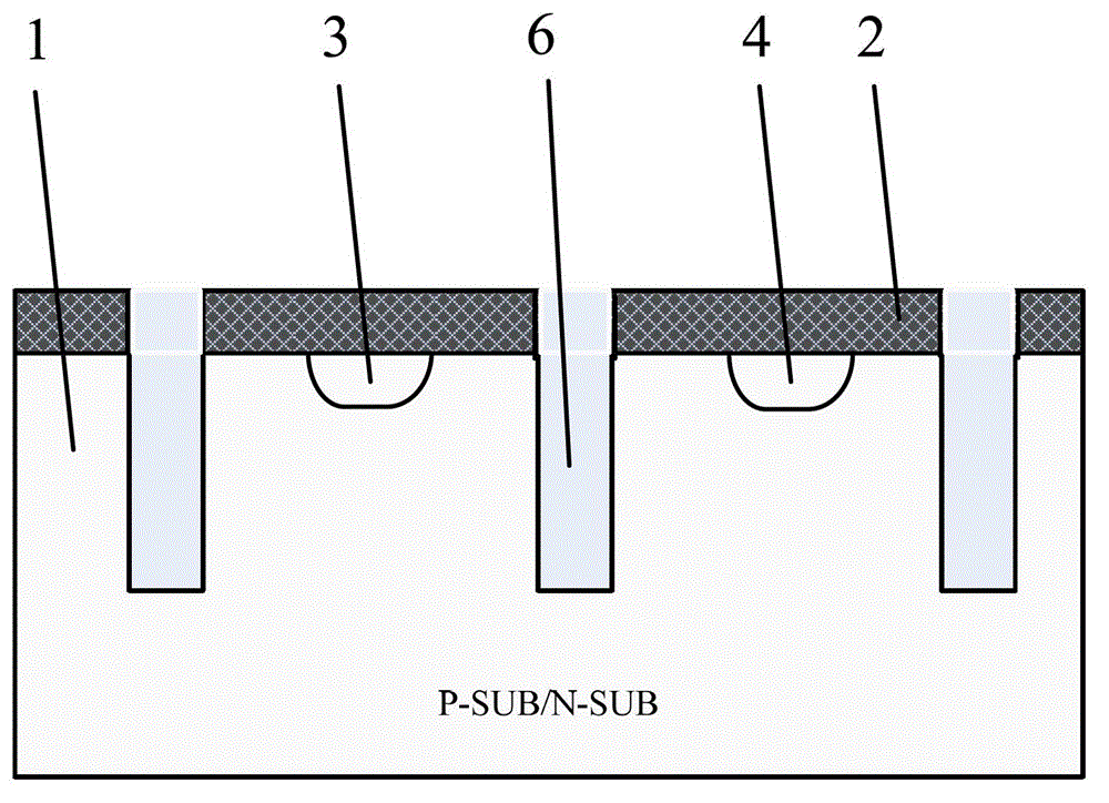
[0040] (2) On the silicon wafer forming the N-type buried layer 3 and the P-type buried layer 4, etch the deep groove 6, oxidize the sacrificial layer, oxidize the barrier 7, deposit polysilicon 8 and CMP polysilicon 9 to form dielectric isolation Area:
[0041] First, a dielectric isolation groove ...
PUM
| Property | Measurement | Unit |
|---|---|---|
| thickness | aaaaa | aaaaa |
| width | aaaaa | aaaaa |
Abstract
Description
Claims
Application Information