Manufacture method of all-dielectric isolation silicon on insulator (SOI) material sheet for complementary bipolar process

A bipolar process and manufacturing method technology, applied in semiconductor/solid-state device manufacturing, electrical components, circuits, etc., can solve problems such as pattern drift, poor consistency of active layer parameters, and achieve good consistency, low production cost, and omission of Effects of Epitaxy Process

Active Publication Date: 2013-07-10
NO 24 RES INST OF CETC
View PDF4 Cites 1 Cited by
  • Summary
  • Abstract
  • Description
  • Claims
  • Application Information

AI Technical Summary

Problems solved by technology

[0005] In order to overcome the problems of stacking faults and slip lines in the active layer of the SOI material sheet made by the above-mentioned background technology, poor consistency of active layer parameters, and pattern drift after epitaxy, the present invention proposes an all-dielectric for complementary bipolar process A manufacturing method for isolating SOI material sheets, realizing the purpose of fully dielectrically isolated SOI material sheets with low manufacturing costs, fewer active layer defects, good consistency of active layer parameters, and no pattern drift

Method used


Image

  • Manufacture method of all-dielectric isolation silicon on insulator (SOI) material sheet for complementary bipolar process
  • Manufacture method of all-dielectric isolation silicon on insulator (SOI) material sheet for complementary bipolar process
  • Manufacture method of all-dielectric isolation silicon on insulator (SOI) material sheet for complementary bipolar process

Examples


Embodiment Construction

[0036] The method of the present invention will be further described below in conjunction with the accompanying drawings and embodiments. The technical solution of the present invention is not limited to the description of this embodiment.

[0037] The specific manufacturing steps of this embodiment are as follows:

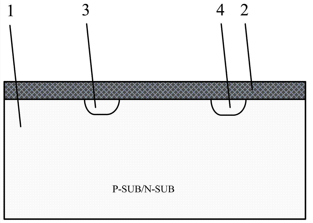
[0038] (1) Fabricate N-type buried layer 3 and P-type buried layer 4 on monocrystalline silicon wafer 1:

[0039] Form a zero-layer mark on the single crystal silicon wafer 1, grow a thin oxide layer 2 with a thickness of 13.5-15.5nm at 950°C, and make an N-type buried layer 3 and a P-type buried layer 4, and anneal at 1050°C for 55 minutes. Such as figure 1 shown.

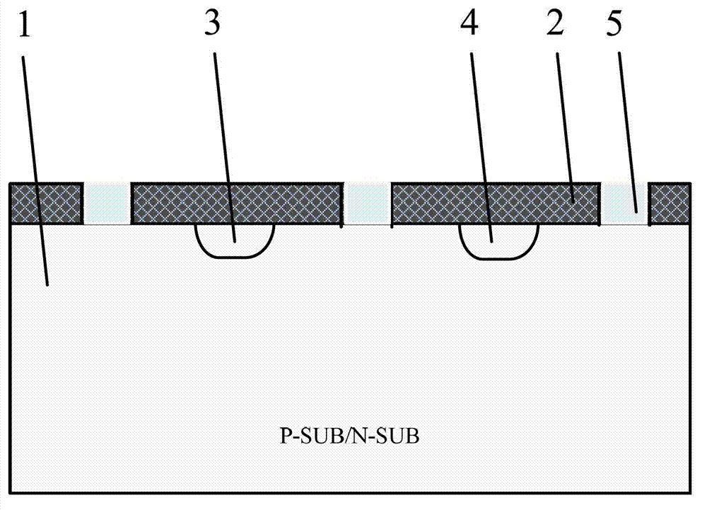
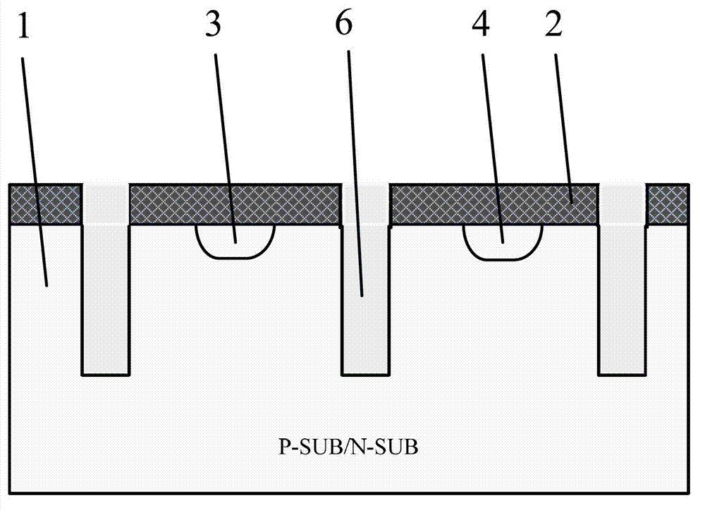
[0040] (2) On the silicon wafer where the N-type buried layer 3 and the P-type buried layer 4 are formed, etch the deep groove 6, oxidize the sacrificial layer, oxidize the barrier 7, deposit polysilicon 8 and CMP polysilicon 9 to form dielectric isolation Area:

[0041] First, a dielectric isola...


PUM


Abstract

A manufacture method of an all-dielectric isolation silicon on insulator (SOI) material sheet for a complementary bipolar process comprises of the steps of manufacturing an N-type buried layer and a P-type buried layer on a first monocrystalline wafer, performing deep-trench etching, sacrificial layer oxidation, trench resistor oxidation and deposition trench filling of polycrystalline silicon and corrugated metal pipe (CMP) polycrystalline silicon on the first monocrystalline wafer to form a dielectric isolation region; arranging a buried oxide layer on a second monocrystalline wafer; performing front silicon bonding of the first monocrystalline wafer with the formed dielectric isolation region and the second monocrystalline wafer with the formed buried oxide layer; and performing reduction and CMP finishing polish of a substrate on the side of the first monocrystalline wafer, and finally forming the all-dielectric isolation SOI material sheet for the complementary bipolar process. The manufacture method has the advantages of being low manufacture cost, few in active layer defects, good in active layer parameter consistency, free of figure drifting and the like, and can be widely applied to the manufacture field of the all-dielectric isolation complementary bipolar process.

Description

technical field [0001] The invention relates to a method for manufacturing an all-dielectric isolation SOI material sheet used in a complementary bipolar process, which is applied to the semiconductor manufacturing field of a complementary bipolar process. Background technique [0002] The complementary bipolar process is one of the most widely used semiconductor manufacturing processes. The conventional dielectric isolation SOI material sheet manufacturing method for the complementary bipolar process is: first make an N-type buried layer and a P-type buried layer on the SOI sheet, and then Produced by growing N-type or P-type epitaxial layers. First of all, the quality of the epitaxial layer is greatly affected by the doping concentration of the buried layer and the defect density of the substrate material itself, and stacking faults and slip lines are prone to occur, and the pattern of the buried layer is prone to large drift after epitaxy; secondly, the epitaxial layer T...

Claims


Application Information

Patent Timeline
Patent Type & Authority Applications(China)
IPC IPC(8): H01L21/762H01L21/8222
Inventor 唐昭焕税国华胡刚毅李儒章王斌张杨波吴建
Owner NO 24 RES INST OF CETC
Why Eureka
Try Eureka