Conformal Mask Packaging Structure and Inspection Method

A packaging structure, conformal mask technology, applied in the direction of single semiconductor device testing, semiconductor/solid-state device testing/measurement, electrical components, etc., can solve the problem of poor substrate cutting, increased material waste, uneven conductive mask layer, etc. question

Active Publication Date: 2015-12-16
UNIVERSAL SCIENTIFIC INDUSTRIAL (SHANGHAI) CO LTD +1
View PDF11 Cites 0 Cited by
  • Summary
  • Abstract
  • Description
  • Claims
  • Application Information

AI Technical Summary

Problems solved by technology

[0003] However, the conformal mask packaging structure is prone to poor shielding performance due to poor substrate cutting, uneven conductive mask layer, or poor connection to the inner ground conductive structure. Therefore, in order to ensure the quality of conformal shielding, the package After the structure is completed, X-ray scanning or crosssection destructive testing must be used to test the shielding effectiveness. In this way, it is necessary to use expensive X-ray scanning equipment, or even destroy the finished product, which increases the cost of materials. Wasteful, so still leaves room for improvement

Method used


Image

  • Conformal Mask Packaging Structure and Inspection Method
  • Conformal Mask Packaging Structure and Inspection Method
  • Conformal Mask Packaging Structure and Inspection Method

Examples


Embodiment Construction

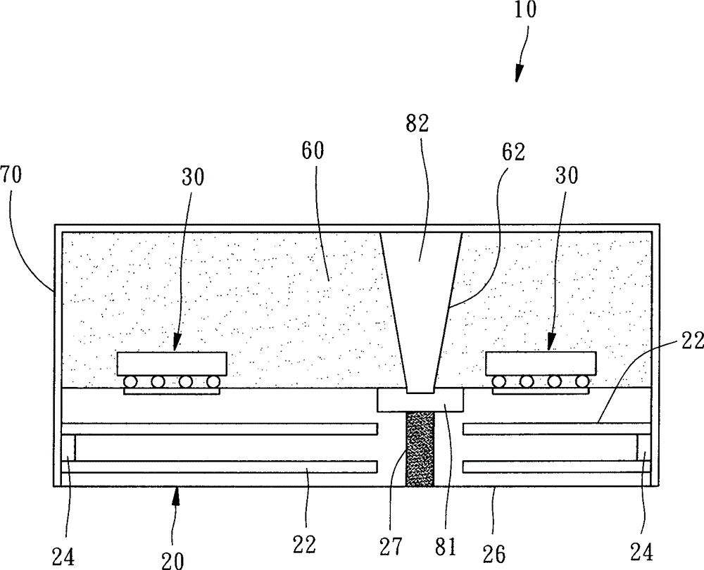
[0019] Please refer to the accompanying drawings, the conformal mask packaging structure 10 provided by a first embodiment of the present invention includes a substrate 20, at least one chip module 30 disposed on the substrate 20, and an encapsulant covering the chip module 30 60, and a conductive mask layer 70 for masking the encapsulant 60, wherein the number of the chip modules 30 is two in this embodiment.

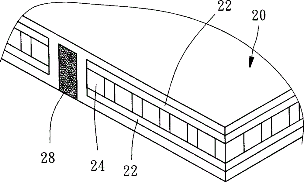
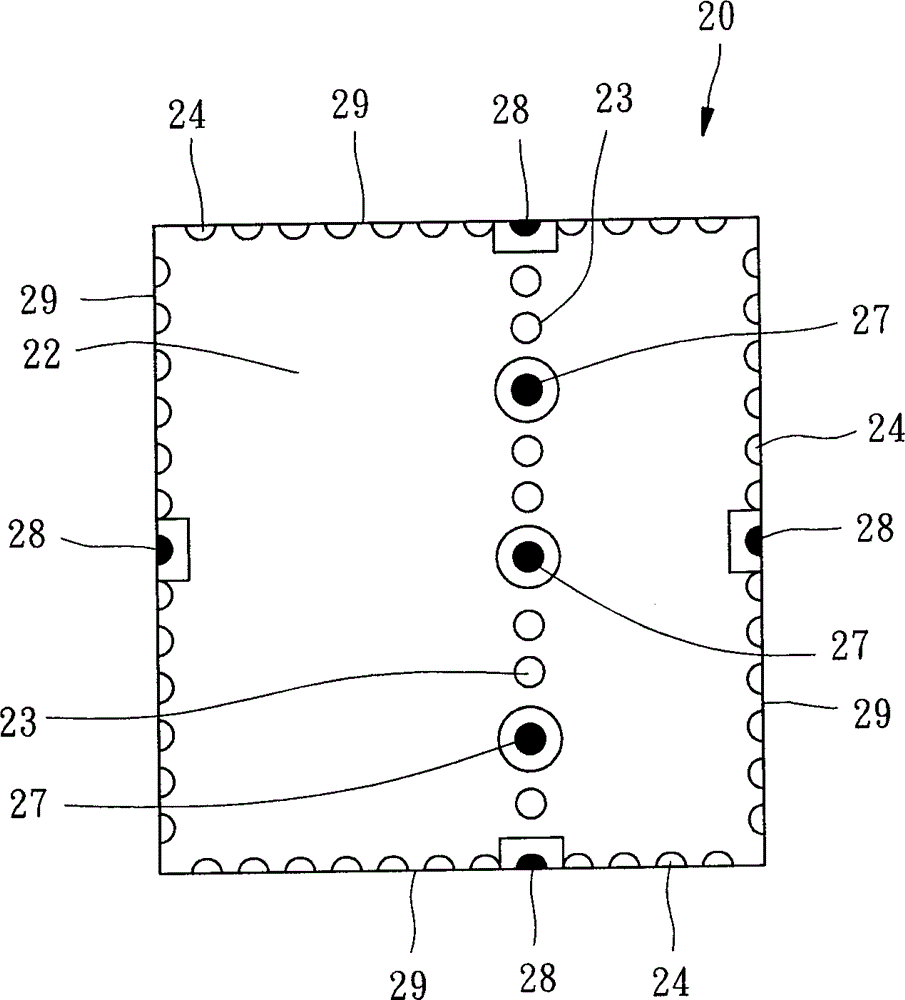
[0020] The substrate 20 is similar to the existing multi-layer printed circuit board, and its inner layer has at least one ground layer 22, and the substrate 20 has a plurality of ground vias (GroundVia) respectively pierced in the printed circuit board and electrically connected to the The inner grounding conductive structures 23, 24 of the grounding layer 22, the aforementioned grounding channels can adopt through holes, blind holes, buried holes or other similar structures and combinations thereof. The inner grounding conductive structures 23, 24 generally refer to c...


PUM


Abstract

A conformal mask packaging structure, comprising a substrate, a chip module arranged on the substrate, a sealant covering the surface of the chip module and the substrate, and a conductive mask layer covering the sealant, the substrate has A plurality of internal ground conductive structures electrically connected to each other, and wherein the plurality of internal ground conductive structures are connected to the conductive mask layer; the package structure is characterized in that the substrate further has at least one exposed independent conductive structure, and the The independent conductive structure is connected with the conductive mask layer. After the packaging structure is manufactured, it is quite easy to measure the resistance value between the independent conductive structure and the conductive mask layer or another independent conductive structure or a grounding point, and judge whether the resistance value is less than a standard value. The electromagnetic mask effectiveness of the package structure was detected accurately.

Description

technical field [0001] The present invention is related to the technology of using conformal shielding to achieve the shielding function of electromagnetic interference (EMI) in the packaging process, in particular to a conformal mask packaging structure and a method for testing its shielding effectiveness The inspection method, and the aforementioned packaging structure and inspection method are also applicable to the situation where both conformal shielding and compartment shielding are used at the same time. Background technique [0002] Conformal mask refers to the formation of a conductive mask layer on the outer peripheral surface of the electronic module by metal sputtering, spraying or other coating methods in the packaging process. Since the module has undergone substrate cutting before coating, it has multiple exposures. The outer inner grounding conductive structure is electrically connected with the inner grounding conductive structure after the conductive mask l...

Claims


Application Information

Patent Timeline
Patent Type & Authority Patents(China)
IPC IPC(8): H01L23/29H01L23/58H01L21/66G01R31/26
CPCH01L2924/181H01L2924/3025H01L2224/16225H01L2924/00012
Inventor 丁兆明刘谦晔姜智浩
Owner UNIVERSAL SCIENTIFIC INDUSTRIAL (SHANGHAI) CO LTD
Why Eureka
Try Eureka