Touch-sensing structure and touch-sensitive device

A technology of touch sensing and touch devices, applied in the field of touch sensing structures and touch devices, can solve problems affecting touch characteristics, large size, and large number of required channels, so as to improve the yield rate of finished products and reduce the Effect of Line Impedance

Inactive Publication Date: 2014-02-12
WINTEK CORP
View PDF5 Cites 21 Cited by
  • Summary
  • Abstract
  • Description
  • Claims
  • Application Information

AI Technical Summary

Problems solved by technology

Therefore, the required number of channels of the single-layer ITO electrode structure 100 is very large, and the larger the size, the required number of channels is even larger. Furthermore, the sensing electrode wiring 106 is located in the display area, so if the impedance needs to be reduced, the The widening of the trace width leads to an excessively large ratio of the overall trace area to the sensing area and affects the touch characteristics

Method used


Image

  • Touch-sensing structure and touch-sensitive device
  • Touch-sensing structure and touch-sensitive device
  • Touch-sensing structure and touch-sensitive device

Examples


Embodiment Construction

[0058] The aforementioned and other technical contents, features and effects of the present invention will be clearly presented in the following detailed description of the embodiments with reference to the drawings. The directional terms mentioned in the following embodiments, such as: up, down, left, right, front or back, etc., are only directions referring to the attached drawings. Accordingly, the directional terms are used to illustrate and not to limit the invention.

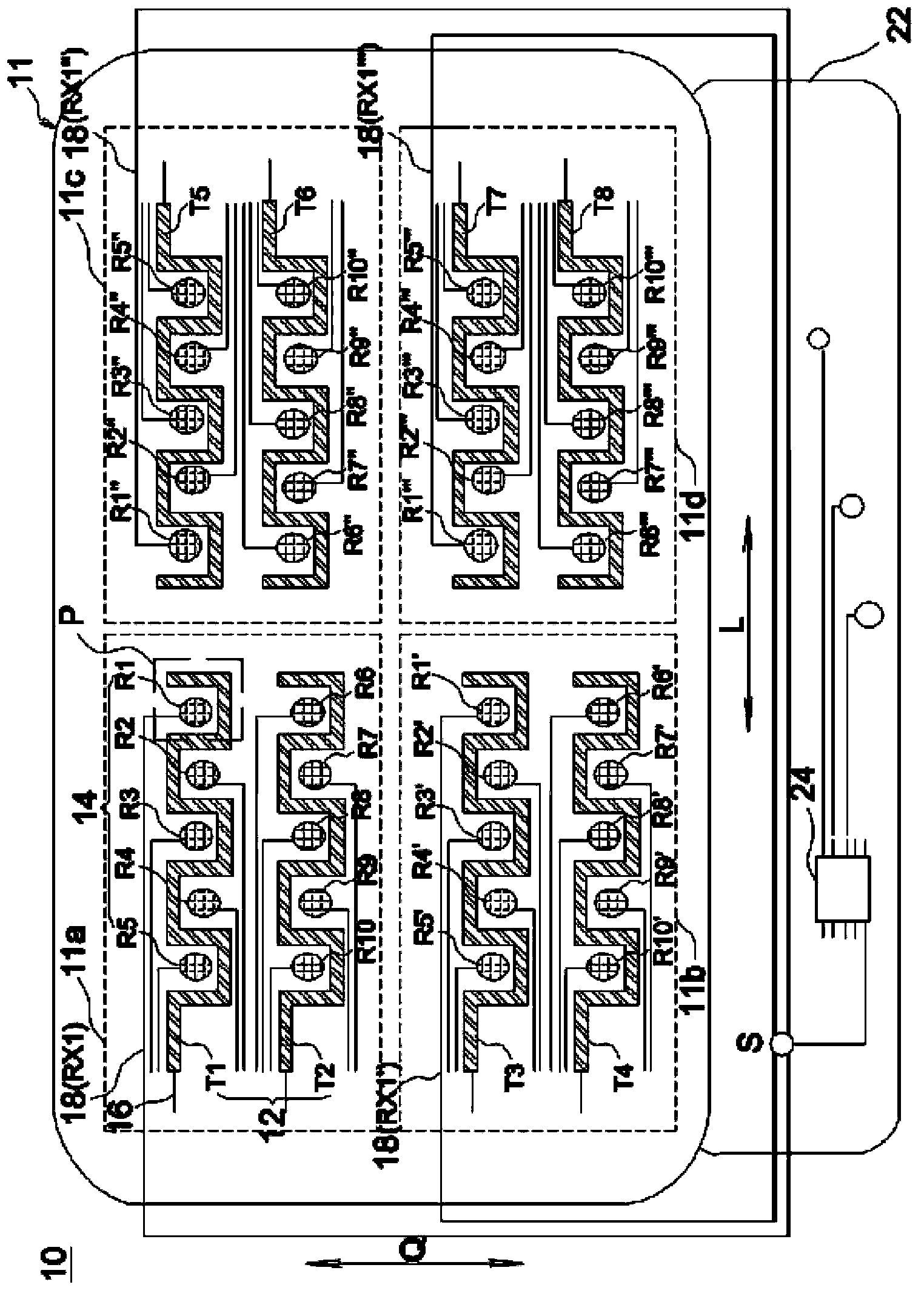
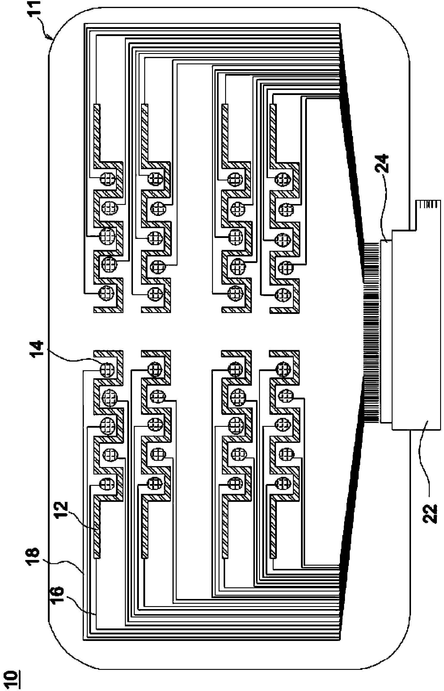
[0059] figure 1 It is a schematic diagram of a touch sensing structure 10 according to an embodiment of the present invention. According to the design of an embodiment of the present invention, the touch sensing structure 10 is a single-layer electrode structure. The touch sensing structure 10 may include a substrate 11 and a transparent conductive layer distributed on a surface of the substrate 11, and the transparent conductive layer may include a plurality of first electrodes 12 and a plurality of se...


PUM


Abstract

A touch-sensing structure includes a substrate and a conductive layer. The conductive layer spreads over a surface of the substrate and includes a plurality of first electrodes, a plurality of second electrodes, a plurality of first conductive lines, and a plurality of second conductive lines. The surface is divided into a plurality of regions. The second electrodes are divided into multiple second electrode groups, and each second electrode group is formed by at least one of the second electrodes in each of the regions. Each of the first conductive lines is connected to one of the first electrodes, and each of the second conductive lines is connected to one of the second electrodes. The second conductive lines connected to the second electrodes in the same second electrode group are electrically connected with each other.

Description

technical field [0001] The invention relates to a touch sensing structure and a touch device. Background technique [0002] Currently, the touch sensing structure of the capacitive touch device is usually formed by double-side ITO (double-side ITO) or single-side ITO (single-side ITO) process. In a double-sided ITO process, it is necessary to perform coating and lithographic etching processes on both sides of the glass substrate to form X-axis and Y-axis sensing electrodes on both sides of the glass substrate. It is easy to cause the yield rate to drop. In addition, in a single-sided ITO process, the X-axis and Y-axis sensing electrodes are formed on the same side of the glass substrate. Due to the need for cross-bridge structure design in the plane, the X-axis and Y-axis sensing electrodes are prone to instability due to the material properties of the organic insulating layer. or other factors causing short circuit or open circuit problems. Therefore, another single-laye...

Claims


Application Information

Patent Timeline
Patent Type & Authority Applications(China)
IPC IPC(8): G06F3/044
CPCG06F3/0443G06F3/0448G06F3/04164H10K50/805
Inventor 陈国兴陈昱廷苏国彰苏振豪
Owner WINTEK CORP
Why Eureka
Try Eureka