Broadband Panel Array Antenna

An array antenna, flat panel technology, applied in antennas, antenna arrays, resonant antennas, etc., can solve the problems of negative growth, decrease in gain bandwidth, unfavorable miniaturization, etc., and achieve the effect of widening bandwidth, increasing gain, and being conducive to miniaturization.

Active Publication Date: 2015-12-09
成都宁锦威通信技术有限公司
View PDF7 Cites 2 Cited by
  • Summary
  • Abstract
  • Description
  • Claims
  • Application Information

AI Technical Summary

Problems solved by technology

The 1dB gain bandwidth of the array can reach 6%, but considering that its feed adopts a series feed structure, its gain bandwidth will gradually decrease as the array antenna diameter increases; in addition, its feed structure has a large area, which is not conducive to miniaturization , it is difficult to form a large array to achieve high gain
[0006] From the existing reports, it can be found that although the substrate-integrated waveguide has advantages in millimeter-wave antenna and array design, it does not solve the contradiction between high gain and wide frequency band. , broadband characteristics, more difficult
In addition, there is an actual need to further increase the gain. Considering that the dielectric loss of the long substrate integrated waveguide at the millimeter wave frequency is also considerable, the gain increase brought by the increase in the number of antenna elements will be offset by the loss caused by the increase in the length of the feeder. , or even negative growth

Method used


Image

  • Broadband Panel Array Antenna
  • Broadband Panel Array Antenna
  • Broadband Panel Array Antenna

Examples


Embodiment 1

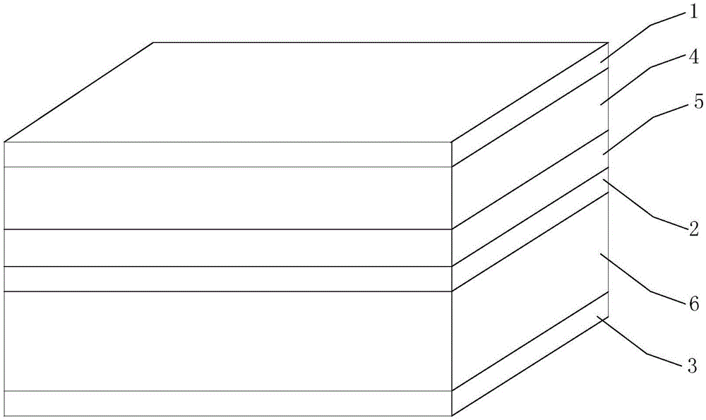
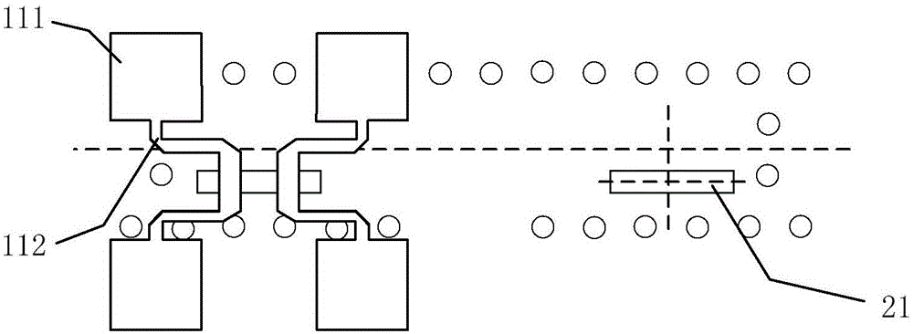
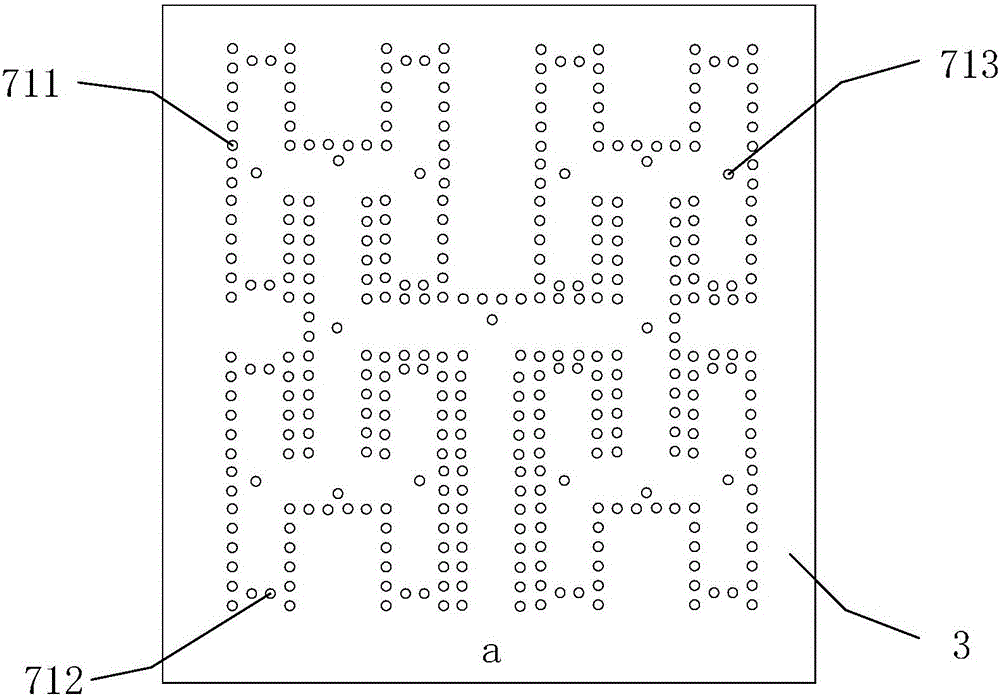
[0032]In this embodiment, the array of the broadband panel array antenna is a 4×4 array, and its center frequency is 61.5 GHz, and an electromagnetic full-wave simulation is performed on it in HFSS. The broadband panel array antenna includes a first metal copper-clad layer 1, a first dielectric layer 4, a second metal copper-clad layer 2, a second dielectric layer 6, an adhesive layer 5, a third Metal copper-clad layer 3, etched on the first metal copper-clad layer 1 are multiple groups of microstrip sub-arrays 11, and each group of microstrip sub-arrays 11 is composed of two microstrip patch units 111 and two microstrip patch units connected to each other. The microstrip feeder 112 of the chip unit 111; the second dielectric layer 6 is provided with a "I"-shaped substrate integrated waveguide feeding network, and the substrate integrated waveguide feeding network includes a plurality of substrate integrated waveguide units and power The sub-tuning hole 713, the substrate inte...

Embodiment 2

[0034] In this embodiment, the array of the broadband panel array antenna is a 32×32 array, and its center frequency is 61.5 GHz, and an electromagnetic full-wave simulation is performed on it in HFSS. The broadband panel array antenna includes a first metal copper-clad layer 1, a first dielectric layer 4, a second metal copper-clad layer 2, a second dielectric layer 6, an adhesive layer 5, a third Metal copper-clad layer 3, etched on the first metal copper-clad layer 1 are multiple groups of microstrip sub-arrays 11, and each group of microstrip sub-arrays 11 is composed of two microstrip patch units 111 and two microstrip patch units connected to each other. The microstrip feeder 112 of the chip unit 111; the second dielectric layer 6 is provided with a "I"-shaped substrate integrated waveguide feeding network, and the substrate integrated waveguide feeding network includes a plurality of substrate integrated waveguide units and power The sub-tuning hole 713, the substrate i...


PUM


Abstract

The invention discloses a broadband flat plate array antenna, broadband can be achieved, and array antenna gain can be improved. According to the broadband flat plate array antenna, a coupling groove is used for stimulating two micro-strip subarrays, at the time, the impedance of a single micro-strip wire is high, a radiation paster can easily carry out high-impedance matching, accordingly the bandwidth of the micro-strip subarrays is widened, broadband is achieved, the relative bandwidth (Sll < -10 dB) of the feeding mode can reach 16%, 1 dB gain bandwidth can reach 14.6%, and common structure bandwidth is only about 6%. In addition, an H-shaped base chip is used for integrating a waveguide feeding network, the micro-strip subarrays are connected in parallel for feeding, along with increasing of array units, the bandwidth is hardly changed, broadband features can be kept in a large array, and array antenna gain can be improved gradually. In addition, the feeding network is placed below the micro-strip subarrays, extra circuit area cannot be increased, and array antenna miniaturization is promoted. The broadband flat plate array antenna is suitable for promotion and application in the technical field of microwave and millimeter wave antennas.

Description

technical field [0001] The invention relates to the technical field of microwave and millimeter wave antennas, in particular to a broadband flat panel array antenna. Background technique [0002] In wireless communication systems, antennas are key components for signal reception and transmission. With the development of wireless mobile communication technology, microwave and millimeter wave antennas are required to achieve low-profile, high-gain, and wide-band characteristics as much as possible while ensuring electrical performance. [0003] The implementation of low-profile antenna mainly includes printed antenna and waveguide slot antenna. The printed antenna has small thickness, light weight, and is easy to conform to the installation carrier; the disadvantage is that the feeder has a large loss at millimeter wave frequencies, and it is difficult to achieve high gain. The waveguide slot antenna has high radiation efficiency and is easy to realize beam forming; the disa...

Claims


Application Information

Patent Timeline
Patent Type & Authority Patents(China)
IPC IPC(8): H01Q9/04H01Q13/08H01Q21/00
Inventor 程钰间吴杰黄伟娜刘小亮
Owner 成都宁锦威通信技术有限公司
Why Eureka
Try Eureka