Lamination packaging structure of double chips

A stacked packaging, dual-chip technology, applied in the direction of semiconductor/solid-state device parts, semiconductor devices, electrical components, etc., can solve the problems of limiting the function of finished circuits, waste, etc., to increase the assembly volume of components and improve the function of the package body , Conducive to the effect of product volume

Inactive Publication Date: 2014-06-04
XIAN WEIZHENG ELECTRONICS SCI & TECH
View PDF0 Cites 0 Cited by
  • Summary
  • Abstract
  • Description
  • Claims
  • Application Information

AI Technical Summary

Problems solved by technology

[0002] The traditional chip packaging technology is all for single-chip packaging. There is only one chip in a ceramic shell. On the one hand, it limits the function of the packaged finished circuit, and on the other hand, it also causes a lot of waste.

Method used


Image

  • Lamination packaging structure of double chips

Examples


Embodiment Construction

[0008] The present invention will be described in more detail below in conjunction with the accompanying drawings and embodiments.

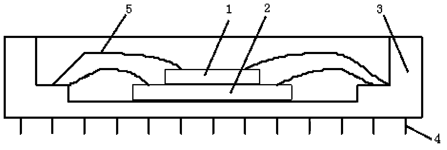
[0009] As shown in the figure, the present invention is a two-chip stacked packaging structure, including a large chip 2 and a small chip 1, and the reverse side of the large chip 2 is pasted on the inner bottom of the ceramic package shell 3 through conductive glue or insulating glue. The reverse side of the small chip 1 is pasted on the front of the large chip 2 by insulating glue, and the lead-out ends of the small chip 1 and the large chip 2 are pressure-welded on the ceramic package shell 3 through gold wire 5 and lead out through the pin 4 .

[0010] There are more chips in the same package. Its functions have been expanded, and this way does not need to develop new chips again, which effectively reduces the development cost and cycle.


PUM


Abstract

The invention provides a lamination packaging structure of double chips. The lamination packaging structure comprises the big chip and the small chip. The back surface of the big chip is attached to the inner bottom of a ceramic packaging shell through a conductive adhesive or an insulating adhesive, the back surface of the small chip is attached to the front surface of the big chip through an insulating adhesive, and the leading-out terminal of the small chip and the leading-out terminal of the big chip are both arranged on the ceramic packaging shell in a bonding mode through a golden wire and are led out through pins. According to the lamination packaging structure of the double chips, the double chips are packaged into the same structure, and a chip with more powerful functions is formed. According to the scheme, the function of a packaging body can be effectively improved, and due to the lamination mode, the assembly quantity of components is increased by two times under the condition that the area is not changed, and the reduction of the size of a product is facilitated.

Description

technical field [0001] The invention relates to the technical field of bare chip packaging, in particular to a double-chip stacked packaging structure. Background technique [0002] The traditional chip packaging technology is all for single-chip packaging. There is only one chip in a ceramic shell. On the one hand, it limits the function of the packaged finished circuit, and on the other hand, it also causes a lot of waste. Contents of the invention [0003] In order to overcome the disadvantages of the above-mentioned prior art, the object of the present invention is to provide a two-chip stacked packaging structure. [0004] In order to achieve the above object, the technical scheme adopted in the present invention is: [0005] A two-chip laminated packaging structure, including a large chip 2 and a small chip 1, the reverse side of the large chip 2 is pasted on the inner bottom of the ceramic packaging shell 3 through conductive glue or insulating glue, and the revers...

Claims


Application Information

Patent Timeline
IPC IPC(8): H01L25/00H01L23/488
CPCH01L2224/32145H01L2224/48091H01L2224/73265H01L2924/00014
Inventor 李佳
Owner XIAN WEIZHENG ELECTRONICS SCI & TECH
Why Eureka
Try Eureka